- Products & Capabilities

- About
- Resources
PCB Trace: Backbone of PCB Design


PCB trace technology is crucial for modern electronics, ensuring reliable and efficient signal transmission. Key elements include trace width, spacing, and material selection.
PCB trace technology forms the backbone of modern electronic design through which run the convoluted paths that interconnect components on a printed circuit board. These conducting tracks play a great role in transmitting electrical signals with high accuracy and speed throughout the circuit. The performance, reliability, and functionality of an electronic device depend to a large extent on the design and quality of the PCB traces. Due to the fact that devices are getting smaller and more complex, this area of precision and innovation in PCB trace technology plays a very important role in everything, from consumer electronics to advanced systems within an industrial setting.
The Basics of PCB Traces
These allow engineers to design high-performance PCBs by understanding the basic trace width, layout, and material properties of a PCB trace. Knowing the fundamentals of a trace will enable better signal integrity, minimal EMI, and good thermal management. Good thermal management equates to a more reliable and efficient electronic design.
Important Concepts and Components
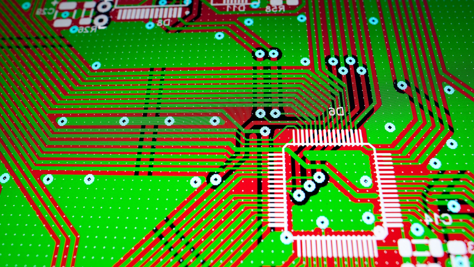
Traces
Traces are the conductive paths etched on the substrate, usually made from copper due to its good conductivity and durability. These paths are designed with a lot of consideration to have specific widths and thicknesses for carrying different levels of current to maintain impedance for signal integrity. Advanced technologies, such as HDI- High density interconnect technologies, provide more intricate and compact designs.
Pads
Pads are areas of exposed copper that form locations where components are soldered. There are mainly two types: through-hole pads for components whose leads pass through the board, and surface mount pads for components that are placed directly on the surface of the PCB. Pads are so important to be able to create stable connections and also guarantee the best conductivity.
Vias
Vias are plated through-holes that connect different layers of a multi-layer PCB by which complex circuits requiring vertical signal routing can be developed. These can be through-hole, blind (outer to inner layers), or buried (inner layers not reaching outer surfaces). Microvias in HDI PCBs have done much to allow even more miniaturization and sophistication.
The Function and Importance of PCB Traces
Conductor traces are where the electrical signals travel from one component to another in an electronic circuit. They make for good and reliable signal transmission, generally quite critical for device performance. In the case of an amplifier circuit, the traces will now connect the power supply, the input signal, and the transistors to the output to make sure amplification occurs correctly. Trace design needs to be done very carefully because a single mistake in it may give rise to errors in performances or even complete failures.
Materials and Construction of PCB Traces
Material Selection
Copper is the most common conductor used for traces on PCBs because of its superior electrical and thermal conductivity, allowing less resistive losses and hence better power distribution. Other materials used for traces include aluminum and silver, with specialized uses. Aluminum has higher strength-to-weight ratios and better thermal conductivity hence finds applications in power electronics; silver is used in radio-frequency and high-frequency circuits due to its higher conductivity despite it being more expensive.
Manufacturing Processes
Photolithography
The process of photolithography involves coating the copper-clad board with a photoresist layer, exposing it to ultraviolet light through a photomask, developing the exposed areas in order to create a patterned layout, and finally etching the developed pattern into the copper layer.
Electroplating
With the purpose of adding more thickness to copper traces and other conductive layers, hence improving electrical properties and giving them mechanical durability, electroplating is carried out.
Factors Affecting Quality
Some of the factors that affect the quality of the PCB trace include:
Copper Thickness: Ranges from 0.5 oz/ft² to 2 oz/ft², where the changes in thickness impact current-carrying capacity and thermal performance.
Surface Finishes: Hot air solder leveling, immersion gold, and organic solderability preservatives for solderability and corrosion resistance.
Design Considerations for Effective PCB Traces
Trace Width
This is a main parameter that influences current-carrying capacity and resistance. With wider traces, higher currents can be carried at lower resistance, and this is critical in power delivery to minimize voltage drops. The minimum trace width according to the IPC-2221 depends on the required current and thermal demands that include ambient temperature.
Trace Spacing
Adequate trace spacing prevents cross-talk and EMI, which supports the signal integrity of high-frequency circuits, as interference with signals in such systems may lead to corrupted data and other malfunctions.
Layout Considerations
The strategic design of the layout optimizes the routing of both signals and power lines, reduces the lengths of signal paths, shrinks possible interference, and improves thermal management. The designer also has to plan for component placement regarding effective connectivity and mechanical stability.
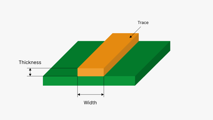
Trace Resistance
Trace resistance determines signal transfer loss and power dissipation. The trace resistance can be calculated using the formula,
Resistance = Resistivity × Length / Area × (1 + (Temp Co × (Temp - 25)))
Where Area is given by Thickness × Width. For the correct estimation of power loss, correct calculation of trace resistance is a must for efficient PCB design.
Trace Current
The current capacity over a PCB trace is the maximum it can carry without causing damage to an electronic component. It would be determined by trace width and thickness. Properly designed traces prevent overheating and ensure reliable operation of the PCB.
Conclusion
It will be fair to describe the traces of the PCB as central to the modern electronics' functionality. Understanding the trace design basics, material selection, and manufacturing processes; consideration for trace width and spacing; resistance-all of these play a big role in effective and reliable PCB design. Designers are able to ensure, by paying heed to the industry's strict standards and availing themselves of advanced technologies, that the PCBs meet rigorous demands from today's electronics.
At PCBX, we strive to be your leading partner in high-quality PCB solutions to meet your needs. Our very skilled team in the design and manufacture of printed circuit boards assures dependable and effective performance of any electronic equipment. We thus welcome any questions you may have or specifications you might have for your PCB projects. Please consult our experts for consultation.
Hot Tags:

Contact us

If you can't find what you're looking for, please contact us.
Article
Pads and vias are crucial for PCB design: pads serve as soldering points for components, while vias connect different layers. Understanding and correctly implementing them ensures reliable, efficient, high-performance PCBs.
 2024/09/16
Vias—blind, buried, and through-hole—are essential in multi-layer PCBs, enabling signal and power transfer between layers. Covering techniques like tenting and plugging with solder masks enhance PCB reliability and performance, crucial for compact designs.
2024/09/11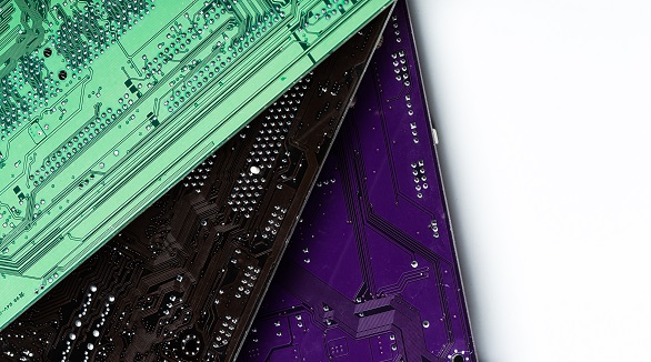
PCBs (Printed Circuit Boards) are fundamental in electronics, composed of multiple layers like silkscreen, soldermask, copper, and substrate, chosen for specific electrical functions.
2024/08/07