- Products & Capabilities

- About
- Resources
Pin in Paste (PiP) Soldering Technology


Pin in Paste (PiP) enables efficient, cost-effective PCB assembly, integrating through-hole and surface mount components in a single reflow pass, reducing costs.
With the ever-changing world of electronics assembly, the demand for low-cost, effective, and dependable assembly procedures is greater than ever. With evolving technology, the demand to assemble through-hole and surface mount parts onto printed circuit boards (PCBs) without a problem is greater than ever. Pin in Paste (PiP) soldering technology is an innovative assembly procedure that has revolutionized everything. With its case for flexibility and efficiency, PiP is the solution of choice for assembly lines in our current age. Technicality, procedure, advantages, and points to consider when it comes to PiP soldering technology are investigated by this article.
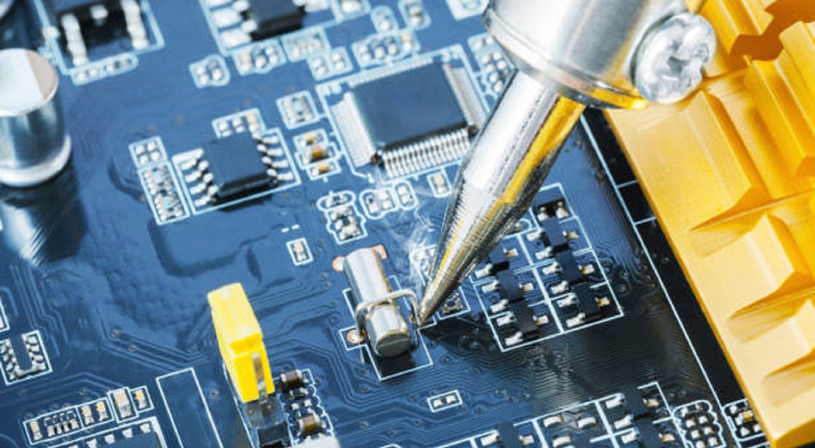
Pin in Paste soldering replaces PCB assembly by allowing through-hole and surface mount devices to be soldered simultaneously with a single reflow process. It is done by depositing solder paste directly into through-hole vias and pads before component assembly, streamlining the whole assembly process. Through-hole devices once required separate wave or selective soldering processes, but PiP skips these additional steps, which simplifies production and makes it cheaper.
Key Steps in the PiP Process
Precise Solder Paste Dispensing
It begins with precise solder paste dispensing into the through-holes of the PCB. It uses extremely high precision dispensing machines to attain the precision for dispensed accuracy and to place the exact paste volume to attain long-lasting solder joints.
This is a very important step that opens the way for component soldering correctly and removes defects due to less or more paste.
Component Placement
Components are subsequently mounted onto the board following solder paste application by advanced pick-and-place machinery. The paste acts as a temporary adhesive, holding components in position until reflow soldering.
In some cases, additional adhesive material is required to prevent parts from moving, particularly for bigger or irregularly weighted pieces.
Reflow Soldering
Subsequently, the PCB assembly undergoes reflow soldering. The entire board is heated during this procedure, melting the solder paste and forming strong, long-lasting bonds between the PCB and component pins.
For through-hole and surface mount components to be soldered as well as possible, the reflow profile needs to be carefully managed, often using lead-free solder pastes like SAC305.
Why Opt for Pin in Paste Soldering?
PiP technology is highly appealing for a variety of applications since it provides several benefits over conventional through-hole soldering methods.
Decreased Capital Expenditures: PiP lowers the capital costs associated with production lines by eliminating the requirement for wave or selective soldering equipment. Significant cost reductions result from this, particularly for producers who create low-to-medium volume, high-mix manufacturing runs.
Enhanced dependability: By avoiding extra soldering passes that might compromise component dependability, PiP reduces thermal shock. It offers electronic assemblies that are more robust and long-lasting.
Enhanced Design Freedom: There is no greater design freedom when through-hole and surface mount components are able to be assembled on the same board. It enables more intricate, small electrical designs and streamlines product design.
Simplified Procedure: By incorporating through-hole soldering into the SMT reflow process, PiP shortens cycle times and production procedures. Faster manufacturing turnarounds and increased productivity are made possible by the optimized process.
Greater Density Capability: PiP printing enables the insertion of components at densities higher than wave soldering can do, resulting in more intricate assemblies that can take advantage of the current shrinking trends.
Better Quality: Through its single-pass reflow, PiP realizes lower defect rates and improved consistency of joint quality over traditional processes like wave or selective soldering.
Considerations in the Implementation of PiP Processing
Effective utilization of PiP soldering includes taking into consideration some very important factors:
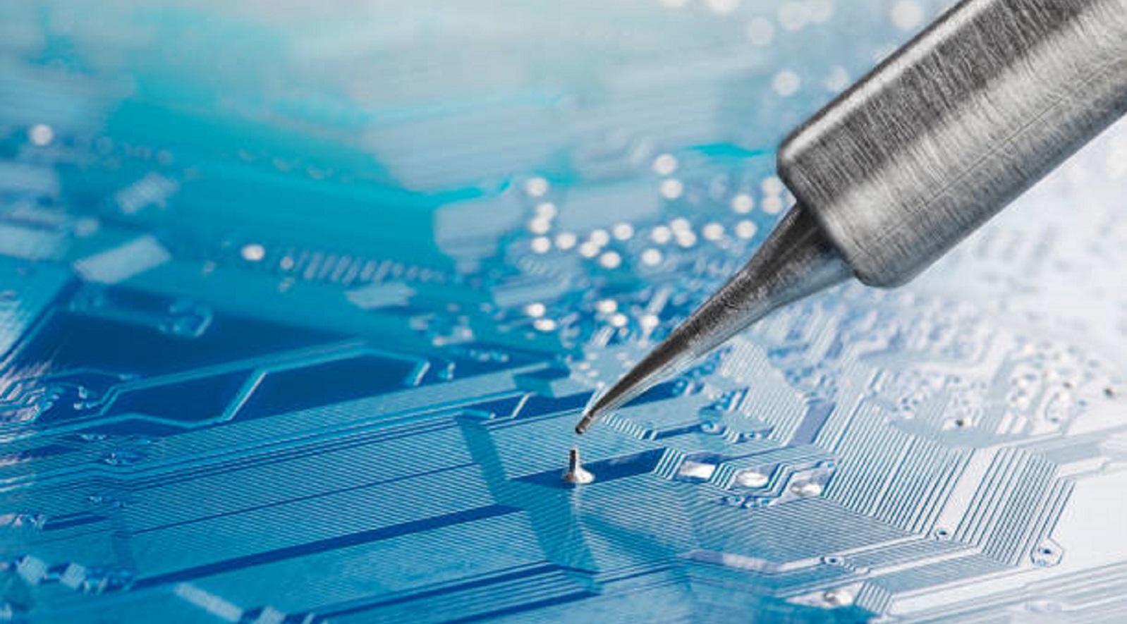
Paste Deposit Accuracy: Paste solder dispensing accuracy is extremely important. It must be deposited cleanly within the holes without displacement or smearing during placement in a bid to avoid defects and joint integrity.
Component Pitch and Hole Preparation: While PiP can handle fine-pitch components, it has problems handling ultra-fine pitches. Besides, surface treatments such as plasma treatment might be necessary in order to facilitate solder wetting to hole walls.
Reflow Profiling: Accurate reflow profiles with potential dual-speed profiles with longer soak above the liquidus are essential to achieving consistent soldering results.
PiP Design Guidelines and Applications
For making PiP soldering safe, certain rules of PCB design must be respected. Rules include:
Via Pad Diameters: 0.3mm to 1.0mm is most appropriate in ensuring correct paste deposition and formation of solder joints.
Annular Rings: 0.25mm to 0.5mm rings of holes for mechanical strength are required.
Hole Spacing: Holes should not be three times their diameter away from each other to enable solder paste flow.
Copper Plating: A minimum of 25μm copper thickness needs to be provided for very good electrical performance.
Solder Mask Expansion: An expansion of around 0.05mm to 0.15mm onto pad copper allows for capillary action during soldering.
PiP technology is very convenient for attaching components like switches, transformers, press-fit pins, connectors, and LED displays, which see widespread application in uses ranging from automotive to aerospace electronics.
Balancing PiP Pros and Cons
While PiP offers a lot of benefits, it is not appropriate everywhere:
Advantages:
Lower capital investment
Improved joint quality and reliability
Flexible design versatility and lead-free processing capability
Disadvantages:
Strict process controls are required to avoid risks of tombstoning
Extra step of paste dispensing adds complexity
Issues with ultra-fine pitch components
With the electronics manufacturing sector calling for more sophisticated and reliable assembly processes, PiP is ready to fill these needs. Developments in solder paste materials, dispensing accuracy, and hole preparations are all expanding the application potential of PiP to mixed-technology assemblies. The level of flexibility, cost, and performance are making it a more significant option for the electronics manufacturer if they are going to succeed in the business.
In all, Pin in Paste soldering offers an economical solution to through-hole component assembly without requiring investment in wave or selective soldering equipment. By pre-depositing solder paste in vias and PCB pads, PiP enables soldering to be accomplished in a single reflow pass, in keeping with industry's movement toward leaner, greener manufacturing processes. With growing demand for flexible, high-mix production, PiP is well positioned as an enabler of the future of electronics assembly.
Hot Tags:

Contact us

If you can't find what you're looking for, please contact us.
Article
Box build assembly integrates components into complete systems, including PCBs, cables, and enclosures, requiring careful planning and quality testing.
 2024/12/31
Package on Package (PoP) assembly stacks semiconductor devices vertically, enhancing space efficiency and performance in electronics with design flexibility.
2024/12/20
Tab routing in PCB manufacturing boosts efficiency and quality, ideal for non-linear shapes, offering flexibility, support, and cost-effectiveness in production.
2024/11/05