Power PCB Design
Effective power PCB design ensures high current handling, noise control, thermal management, and safety through specialized layout techniques and component selection.
In the field of power electronics, efficient and reliable PCB design is important. These boards are responsible for delivering and controlling high currents to drive components such as motors, heaters, or batteries. Meeting unique demands involves specialized layout techniques to ensure robustness, safety, and performance. This guide delves into essential principles and practices in power PCB design, focusing on managing high currents, minimizing inductance, thermal design, safety, EMI control, and component selection.
Key Design Considerations
Successful power PCB design involves addressing several key areas to ensure effectiveness and reliability:
High Current Capacity: Use appropriate trace widths, multiple layers, and vias to handle high currents without overheating.
Low Inductance: Shorten loops and interleave supply/return paths to avoid voltage spikes.
Noise Isolation: Partition noise-sensitive sections and employ filtering to control interference.
Thermal Management: Implement thermal reliefs and heatsinks to maintain safe temperatures.
Safety: Design with proper insulation, spacing, and isolation to prevent hazards.
EMI Control: Shielding, filtering, and good signal routing help control noise emissions and immunity.
Reliability: Select components that can support continuous power cycling in addition to transient stresses.
Dealing with High Currents
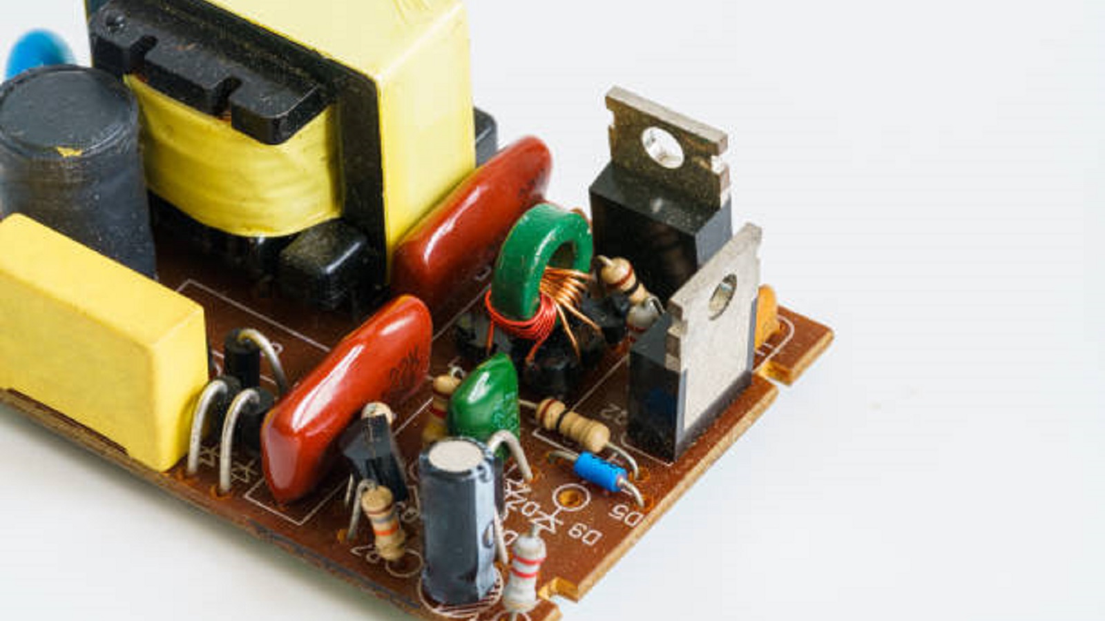
Power electronics can supply hundreds or thousands of amps. Hefty traces are required to carry these currents safely. Here's how:
Thick Traces: Choose the trace widths according to current estimates. For example, 10A may be sufficient with at least 0.5mm (20mil) traces while 50A may require 1mm (40mil) or thicker traces. Consult ampacity tables for an accurate determination.
Distribute Across Layers: Make use of multiple board layers with dedicated power distribution planes as such will allow dividing the current and avoiding trace overload. Use plated through-hole vias for effective conduction between layers.
Incorporate Thermal Relief: Add thermal relief cutouts around traces that connect to inner layers. This will increase the exposed copper surfaces, aiding in localized heat dissipation and enhancing thermal management.
Reducing Parasitic Inductance
Parasitic inductance must be minimized when it comes to dynamic power circuits to avoid damaging voltage spikes:
Short and Direct Paths: Keep the traces short and avoid right angles; if necessary, use 45° angles and prefer curved traces.
Pair and Interleave: Route supply and return traces side-by-side, interleaving pairs to minimize loop area.
Use Copper Fills: Utilize copper fills stitched to the ground plane via closely spaced vias to reduce inductance by disrupting magnetic flux lines.
Eliminate Loops: Avoid loop structures in high di/dt paths; directly connect traces to reduce loop area.
Partitioning for Noise Isolation
Combating noise in power electronics that involve mixed analog and digital circuits requires strategic partitioning:
Use dedicated grounds and power planes to isolate the analog sections from noisy digital areas.
Split planes using isolation gaps and ferrite beads.
Encircle sensitive circuits with guard traces to shield against noise.
Supply input and I/O line filtering to avoid unwanted coupling.
Thermal Design
Many power components operate at high temperatures, requiring active thermal management:
Thermal Pads and Polygons: Utilize broad thermal pads to spread heat from hot components.
Thermal Spokes and Vias: These routes heat efficiently to inner layers.
Direct Connection to Copper: Connect hot components directly to heavy copper areas, a chassis, or heatsinks for dissipation.
Optimal Airflow: Ensure that good ventilation exists around temperature-sensitive components.
Temperature-Resistant Material: The selection of materials should be those capable of withstanding elevated temperatures.
Safety
A designed power system should address the following safety concerns :
Spacing and Insulation: There should be adequate spacing and insulation between high-voltage nodes.
Protection Devices: Include fuses, current limiting resistors, and safe discharge paths.
Compliance Standards: Follow safety standards for enclosure, spacing, insulation, etc.
EMI Control
Switching power electronics generate intensive noise usually, and hence, EMI containment is of much importance for compliance to standards:
Shielding and Grounding: Shielding cans and effective use of grounded copper are necessary to contain emissions.
Filtering Techniques: Feed-through capacitors and ferrite beads would be used for leakage filtering.
Good Layout Practices: Good grounding, decoupling, and bypassing practices.
Current Loop Management: Keep the loops compact and tracks short to minimize EMI.
Component Selection
The selection of proper components is a vital factor in achieving reliability:
Passives
Select high-wattage resistors, high-current inductors, capacitors with high ripple current ratings, and fuses for transient protection.
Common-mode chokes may be used for EMI filtering.
Actives
MOSFETs, IGBTs, and Controllers appropriate for the load
Choose reliable vendors and apply conservative derating
Example Power PCB Implementations
A few examples of good power PCB designs include:
Switch Mode Power Supply: interleaved paths, shielding, thermal relief, and safety spacing all in one.
Power Amplifier: using copper fills, chassis mounting, separating analog/digital sections, and input/output filtering.
Battery Charger: low-inductance traces, dedicated power distribution layers, liberal use of thermal relief.
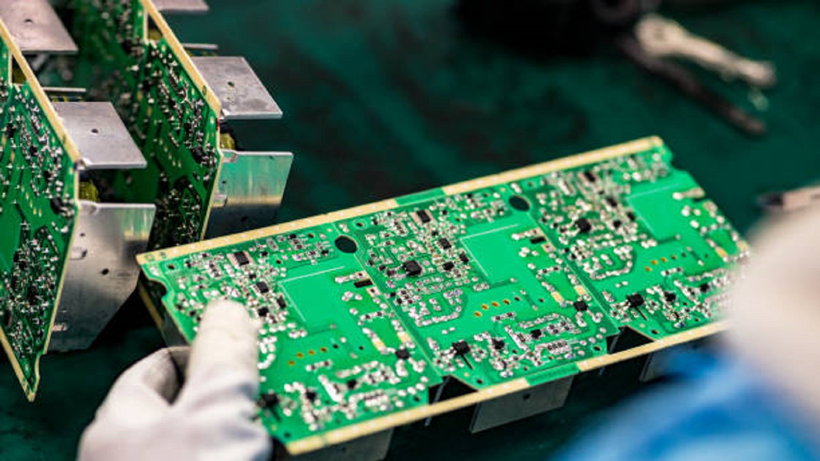
The design of robust power PCBs calls for a holistic approach to current management, inductance minimization, and safe, efficient operation. Application of these best practices and guidelines will enable the engineer to construct a reliable PCB that delivers consistent power under challenging conditions. Power integrity principles are mastered and deployed to deliver dependable, high-performance power solutions that can enable everything from consumer devices to industrial systems.
Hot Tags:
Contact us

If you can't find what you're looking for, please contact us.
Article
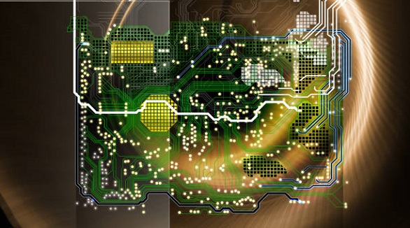
Power and ground planes in PCBs ensure signal integrity, manage heat, and minimize EMI, crucial for efficient, high-performance electronic devices.
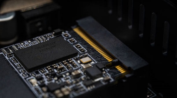
Black FR4 PCBs offer aesthetic and functional benefits, including light blocking, heat dissipation, and enhanced signal performance, suitable for electronics.
DFM ensures cost-effective PCB design by optimizing size, layers, materials, and components, focusing on manufacturability, reliability, and process efficiency.
