- Products & Capabilities

- About
- Resources
Prevent Short Circuits to Ground in QFN Components


QFN components offer size and performance benefits but can cause shorts due to solder bridging, misalignment, and contamination. Prevention includes optimized PCB design, precise assembly, thorough inspection, and effective cleaning.
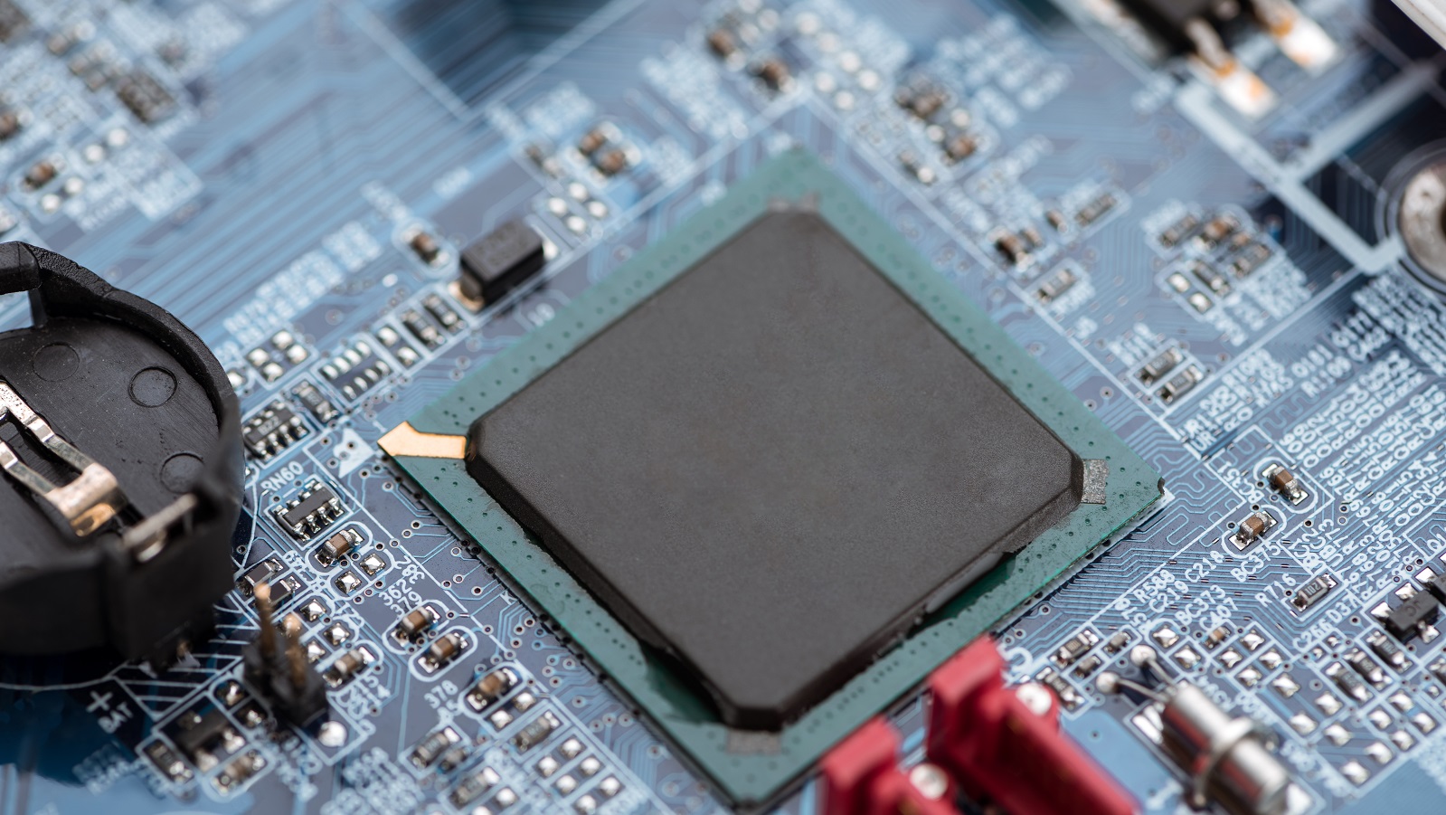
Quad Flat No-Lead (QFN) components come in extremely handy in today's electronics due to their very small size and good performance. A challenge they present, however, is that they can easily create conditions leading to a short circuit to ground. The article is going to look at the root causes of this problem and outline overall ways in which one can prevent occurrences to ensure longevity and the functioning of reliability of electronic design.
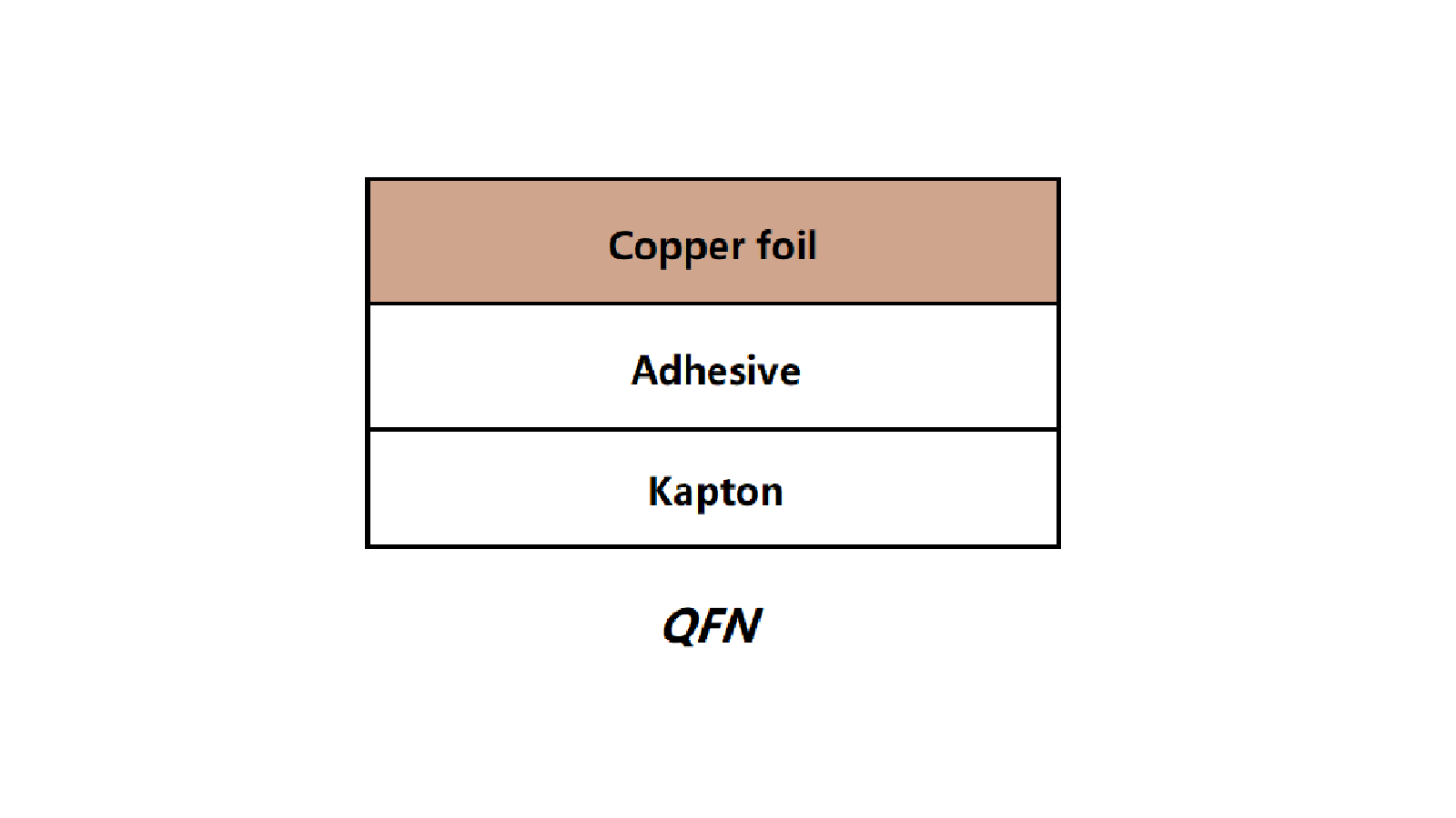
What Are QFN Components?
QFN components are integrated circuit surface-mount packages with the following general characteristics:
Footprint is Smaller: best suited for miniature device designs
Improved Thermal Performance: The devices comprise exposed thermal pads that help them function better thermally.
Superior Electrical Performance: parasitic inductance and capacitance is lower because the connection paths are shorter.
Common Applications
QFN components find extensive applications in:
Mobile and IoT Devices
Automotive Electronics
Consumer Electronics
Industrial Control Systems
Causes of Short Circuits to Ground
Understanding the root causes is key to effective prevention:
Solder Bridging: A condition where excess solder has bridged adjacent pads or a pad and the exposed thermal pad, creating a conductive path.
Component Misalignment: Poor placement during assembly can cause the pins to contact the wrong pads, or the thermal pad.
PCB Design Issues: Insufficient spacing, incorrect pad size, or poorly designed thermal pads increase the possibility of short circuits.
Contamination: Flux residues, moisture, or any other contaminants will easily give rise to unintended conductive paths.
Thermal Pad: Overfilling or underfilling the thermal pad may result in component floating or solder balls and, eventually, in shorts.
Mechanical Stress: Unduly high mechanical stress can result in component warping or cracking, which can yield internal shorts.
Strategies to Avoid Short Circuits
The mitigation of short circuits to ground is multi-faceted:
Optimizing PCB Design
Proper Pad Design: Place manufacturer recommendations on pad layout, spacing, and teardrop pad use for better solder flow.
Thermal Pad Considerations: Stagger the thermal pad, apply a grid of small vias to dissipate heat, and make use of solder mask-defined (SMD) pads for better control.
Ground Plane Design: Use a solid ground plane beneath the QFN component with cutouts to minimize solder bridging.
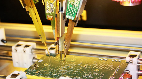
Optimize Assembly Processes
Solder Paste Application: Utilize a high-quality fine-pitch stencil, optimize the solder paste volume, and use of Type 4 or 5 solder paste can be beneficial when pitch devices are finer.
Component Placement: Employ precision pick-and-place machines along with optical alignment systems. Placements should be verified for accuracy before reflow.
Reflow Profile: Develop a particular reflow profile for QFN components, including monitoring and controlling temperature ramp rates to guarantee appropriate peak temperature and time above liquidus.
Rigorous Inspection and Testing
Automated Optical Inspection (AOI): Use high-resolution AOI systems, develop algorithms for QFN inspection, and implement 3D AOI for enhanced defect detection.
X-ray Inspection: Utilize X-ray systems for inspecting occluded solder joints, checking thermal pad solder for voids, internal component integrity. Electrical Testing: Apply in-circuit testing for shorts, functional testing for operation verification and boundary scan testing for increased coverage.
Effective Cleaning and Contamination Control
Flux Selection: Whenever possible, utilize no-clean flux or select fluxes that can easily be removed when cleaning is necessary.
Cleanliness Processes: Utilize efficient flux removal processes for cleaning, using ultrasonic cleaning where required; conduct ionic contamination testing to confirm cleanliness. Storage and assembly areas shall provide humidity control, handle appropriately, and store any moisture-sensitive components in dry environments.
Fiducial Placement: Add fiducial marks for placement accuracy, including local fiducials for critical components.
Testability: Design for testability in order to increase fault detection, and test points should be provided for critical nets.
Conclusion
One of the major challenges that face QFN components is how to avoid any possible short circuit to ground as this will directly affect the integrity and performance of modern electronic devices. The following are comprehensive strategies in PCB design, assembly, inspection, cleaning, and manufacturability that go a long way in helping the manufacturer reduce the risks of short circuits significantly.
At PCBX, we take great experience in the manufacturing of PCBs and Component Assemblies and merge it with Quality and Innovation. For more information or inquiries regarding QFN Component Assembly, please do not hesitate to contact our professional staff. With a team of experts, that is the only way to guarantee the reliability and efficiency of electronic products, and it supports you in succeeding in today's competitive technology world.
Hot Tags:

Contact us

If you can't find what you're looking for, please contact us.
Article
Flying Probe Testing ensures high-performance, durable PCBs and PCBAs by detecting issues like shorts and capacitance mismatches, speeding up production, and reducing costs.
 2024/08/14
As PCB lines and components shrink, traditional visual inspection fails; AOI using DRC and CAD methods is crucial for quality SMT assembly, offering intelligent, accurate inspections.
2024/08/08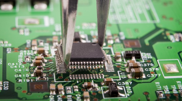
Still, SMT can further feature defects such as solder bridging, cold solder joints, tombstoning, and solder balling. Grasping the very common faults and their solutions is the key toward effective PCB assembly and reducing SMT errors—very much in line with the trend toward PCB miniaturization and higher component density.
2024/07/29