- Products & Capabilities

- Simulation Design & EDA

- About
- Resources
Printed Circuit Boards Glossary and Terminology


Dive into our PCB glossary to master the key terms and definitions essential for efficient design and production, ensuring your projects run smoothly and effectively.
AQL (Acceptance Quality Level) - The highest quantity of defects per 100 units that, on average, can be deemed satisfactory in a process.
Access Holes - A series of holes located in successive strata. Each set shares a common center or axis. The perforations in a multi-layer printed board allow access to the land surface in one of the board's layers.
Activating - This is a procedure that makes nonconductive materials susceptible to electroless deposits.
Additive Process – The deposition or adding of conductive material to a clad or unclad base material.
Ambient – The external environment that interacts with the system or component under consideration.
Analog Circuit - These are circuits that process analog signals (both continuous and variable). This type of circuit produces non-binary output.
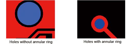
Annular Ring – A conductive substance that entirely surrounds a hole.
AOI - Abbreviation for automated optical inspection, which is a visual examination of circuit boards using a machine scanner to determine workmanship quality by automatically inspecting and analyzing components and solder connections for any defects or anomalies.
Array – A collection of elements or circuits organized in rows and columns on a base material.
Artwork – An precisely sized electronic data configuration utilized to create the artwork master or production master.
Artwork Master – A photographic image of the PCB pattern on film serves to build the circuit board.
Assembly - A collection of parts, subassemblies, or any combination thereof.
Assembly Drawing - A detailed document that provides information on how to place and solder components onto the PCB.
Assembly House - A facility that attaches and solders components to printed circuit boards.
Aspect Ratio - This is the ratio of the PCB thickness to the diameter of the smallest hole.
ATE (Automatic Test Equipment) - The equipment that automatically evaluates functional or static parameters to evaluate performance.
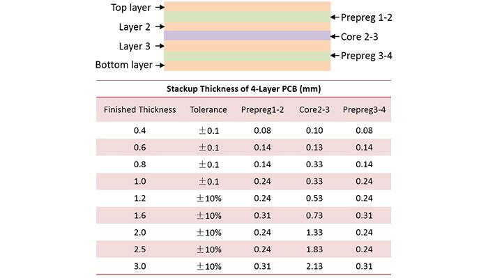
B-Stage – An intermediate step in a thermosetting resin's reaction, where the substance expands and softens when heated, but does not completely fuse or disintegrate when it comes into contact with certain liquids.
Back Drilling - The procedure of making a bigger hole from one or both sides after plating in order to remove the "stub" or unused piece of vias. To reduce the parasitic effects of the via stubs, this is usually necessary in very high speed applications (10GHz or above).
Backplane - A sizable printed circuit board that is used to place modules, connectors, subassemblies, and other printed circuit boards. Traces on the board are used to connect the various components.
Barrel – The cylinder created by coating the walls of a drilled hole.
Bare Board – A printed board that is not assembled.
Base Material – This is the insulating material that forms the electrical pattern. It could be both flexible and rigid. It could be an insulated or dielectric metal sheet.
Base Material Thickness – The thickness of the base material, exclusive of any material applied to the surface or metal foil.
Bed of Nails – A test fixture with a frame and holder that holds a field of spring-loaded pins that come into contact with a planar test item electrically.
BGA (Ball Grid Array) - A leadless array packaging technique wherein the package's underside is mounted with solder balls.
Blind Via – An outside layer of a multilayer printed circuit board is connected to one or more inner layers via a type of via (vertical interconnect access) that does not extend all the way through the PCB to the opposite outer layer.
Blister – An isolated area of swelling and/or separation that occurs between conductive foil and base material, or between any two layers of a laminated base material. It's a type of delamination.
Board Thickness – The total thickness of the conductive material that has been deposited on top of the base material.
Book – A set quantity of inner-layer cores and Prepreg plies constructed for curing in a lamination press.
BOM - A Bill of Materials is a detailed list of the raw materials, components, assemblies, subassemblies, parts, and quantities required to make a product. In the context of electronics and PCB (Printed Circuit Board) manufacturing, a BOM is a precise recipe that guides the assembly and production processes.
Bond Strength – The force per unit area needed to pull two adjacent layers apart using a force perpendicular to the board surface.
Bottom SMD Pads - The quantity of Surface Mount Device pads at the bottom.
Bow – A board's deviation from flatness defined by an approximately cylindrical or spherical curvature such that, if the product is a rectangle, all four corners are in the same plane.
Border Area – The portion of a base material that is external to the end product being manufactured within it.
Buried Via – A via hole drilled through the inner layers of a multilayer board but not into the surface layers.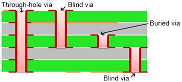
Buried Resistance Board: A printed circuit board with resistors buried inside. This design enhances the integrity of resistive components, hence improving the overall function and reliability of the PCB.
Burr – A ridge that forms around a hole on the exterior copper surface after drilling.
Cable - A cable is a wire that can transfer electricity or heat.
CAD – (Computer Aided Design) – A system in which engineers build a design and see the proposed product on a graphical screen, a computer printout, or a plot. In electronics, the end result would be a printed circuit.
CAE - An abbreviation for computer-aided engineering, which refers to schematic software packages used to create and visualize PCB designs.
Capacitance - The ability of a conductor-dielectric system to store electricity when there is a potential difference between the conductors.
Catalyst – A chemical that initiates or speeds up the reaction between a resin and a curing agent.
Cavity Process - The process of exposing sections of the inner layers. If necessary, the exposed parts can be finished with a soldermask. Typically, any holes in these places must be sealed and capped with copper; prevent holes in exposed areas if feasible.
Center to Center Spacing – The nominal distance on any single layer of a printed board—such as surface mounts and gold fingers—between the centers of neighboring features
Check Plots – Plotted film or pen plots appropriate for client approval of designs and for checking.
Circuit – A collection of interconnected electrical elements and devices that perform a specific electrical purpose.
Clearance Hole – A hole in the conductive pattern that is bigger than and aligned with a hole in the printed board's base material.
Coating - A solid, continuous film that either covers, insulates, or decorates the printed circuit board.
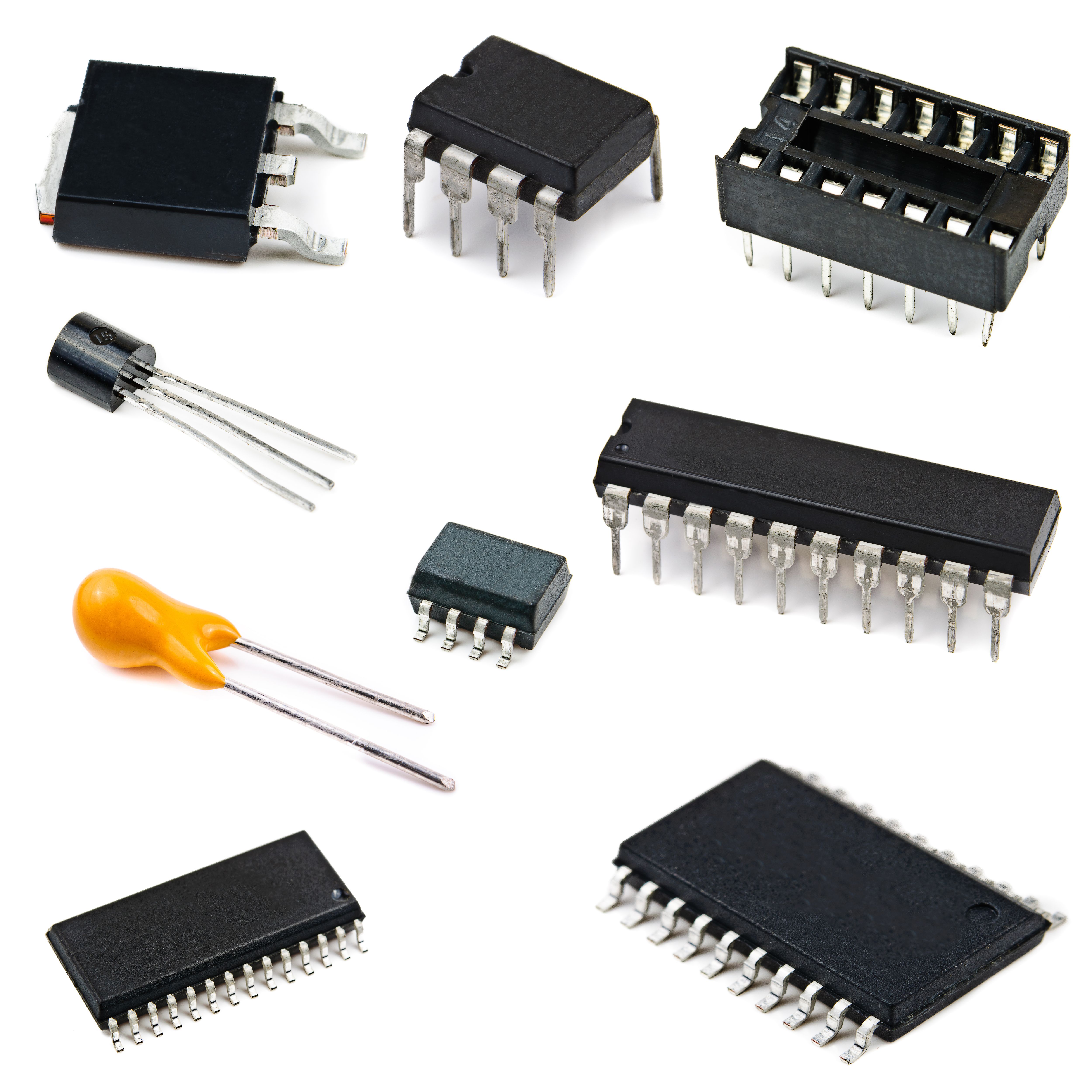
Component – Any of the basic parts used in the manufacture of electronic equipment, such as a resistor, capacitor, DIP, or connection.
Component Hole – A hole used to attach and/or electrically link component terminations, such as pins and wires, to a printed board.
Component Side - Also call "top side", the side of the circuit board where the majority of the components will be found.
Conductive Pattern – The pattern or design of conductive material on a base material. (This comprises conductors, lands, vias, heat sinks, and passive components that are crucial to the printed board manufacturing process.
Conductor Spacing – The visible distance between related edges (not center to center spacing) of isolated patterns in a conductor layer.
Continuity – A continuous path for electrical current to pass in a circuit.
Conformal Coating – An insulating and protective coating that adapts to the shape of the object being coated and is applied to the finished board assembly.
Connector – A plug or receptacle that can be readily connected or disconnected from its counterpart. Multiple-contact connectors bring two or more wires together in a single mechanical assembly.
Controlled Depth Drilling - A process for drilling partially through the thickness of boards.
Controlled Impedance – The process of matching substrate material qualities to trace dimensions and locations in order to provide a precise electric impedance for a signal going down a trace.
Controlled Dielectric – The thickness of the insulating layers between the signal and power or ground planes.
Copper Weight - This phrase refers to the thickness of the copper foil on each layer of a PCB. It is usually given as ounces of copper per square foot.
Countersink Holes - Cone-shaped holes drilled into a printed circuit board (PCB). To allow a countersunk screw to be flush with the PCB surface.
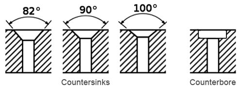
Counterbored Holes - These cylindrical holes are designed to be utilized with a fastener that sits flush with the PCB surface.
Cover Coat - Layer of dielectric that covers the surface (one or both sides) of the board. This can be used when the boards need to be insulated from adjacent conductive surfaces (i.e. heat sinks) or in very high voltage applications.
Crosshatching – The process of dividing a large conductive area into smaller sections by using a pattern of voids in the material.
C-Stage Resin – A resin in the last stages of curing.
CTE – (Coefficient of Thermal Expansion) – The measure of how much a material moves in any axis per degree of temperature change.
Curing – The process of applying heat and pressure to laminate materials to form a bond.
Database – A collection of interconnected data objects stored together with minimal redundancy to serve one or more applications.
Daughter Board - The "daughter" of a "mother" board, a daughter board contains plugs, pins, sockets and connectors and plays a big role in internal connections for electronic devices and computers.
Datum – The theoretically exact point, axis, or plane that serves as the starting point for determining the geometric parameters of a part's features.
Decal - A footprint, is a pictorial depiction of an electronic component.
Design Rule Checking – Using a computer-aided program to verify the continuity of every conductor routing in line with the proper design rules.
Dielectric – A material with a high resistance to the flow current, and which is capable of being polarized by an electrical field.
Digital Circuit - The alternative to an analog circuit. Digital circuits operate in a binary fashion like a switch, exhibiting one of two results as a consequence of an input. This is a typical circuit for computers and similar equipment.
Dimensioned Hole – A hole in a printed board whose position is dictated by physical dimensions or coordinate values that do not always match the specified grid.
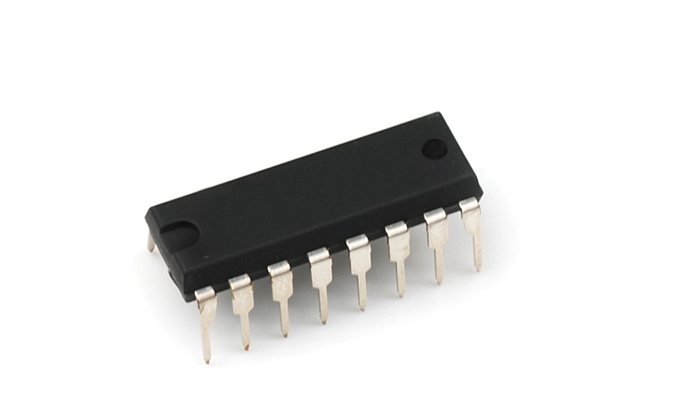
DIP - An abbreviation for a dual in-line package, a DIP is a kind of housing for integrated circuits. This housing will typically come in the form of a molded plastic container with two rows of attachment pins.
Double-Layer PCB - A PCB with traces and pads on both sides rather than just one.

Dry-Film Resists – A coating substance that is specifically designed for use in the production of printed circuit boards and chemically machined items. They withstand a variety of electroplating and etching techniques.
Dry Film Solder Mask – A solder mask film applied to a printed board using photographic methods. This method can manage the higher resolution required for fine line design and surface mount.
Edge Connector - This type of connector is intended for usage on the edge of a PCB and is commonly used to allow the installation of an add-on card.
Edge Plating - Refers to copper plating that extends from top to bottom on a surface or along the edges of a board, allowing for edge soldering and connections.
Electrical Test – Discover how printed circuit boards are tested to assure their quality.
Electroconductive Paste Printed Board - This phrase refers to PCBs made with a silkscreen printing process. To place traces and create stable through-hole connections, an electroconductive printing paste is applied.
Electroplating – The electro-deposition of a metal coating on a conductive object. The object to be plated is placed in an electrolyte and connected to one terminal of a direct current (DC) voltage source. The metal to be deposited is similarly immersed and connected to the other terminal.
EMC - An acronym for electromagnetic compatibility, which refers to a piece of equipment or system's ability to operate without causing excessive electromagnetic interference. Too much electromagnetic interference can disrupt or harm other pieces of equipment in the same electromagnetic environment.
ESD - Abbreviation for electrostatic discharge, which is caused by static electricity.
Etchback – The controlled removal by a chemical process, to a specific depth, of nonmetallic materials from the sidewalls of holes in order to remove resin smear and to expose additional internal conductor surfaces.
Etching – The chemical, or chemical and electrolytic, removal of undesirable sections of conductive or resistive material.
External Layer - Also called an outer layer, an external layer is a layer on the outside of copper to which components attach.
Fabrication Drawing - This drawing allows designers to explain their PCB design to engineers and laborers. It will usually include an image of the board, the locations and details of the holes to be drilled, notes on the materials and procedures used, and so on.

Fiducial Mark – A printed board feature (or features) that is manufactured in the same process as the conductive pattern and serves as a common measuring point for component mounting relative to a land pattern or land patterns.
Fine Pitch - This term refers to chip packages that have micro-spacing between leads of less than 0.050 inch.
Finger - These are metal pads found along the board's edges. These are commonly used when attempting to connect two circuit boards together.
Finished Copper - This is how much copper your board will have on its surface. It is the copper foil thickness, plus plated copper, minus surface preparation. It is given in oz / per sq foot. 1 oz = a minimum of 0.0012”- 0.0014” thickness.
First Article - Refers to the first manufactured board. Before volume production begins, first articles are typically manufactured in small batches so that designers and engineers may evaluate the product for potential mistakes or performance issues.
FR4 - This is a material rating for a flame-resistant material. It also refers to the most commonly used PCB substrate material. The name specifies that the resin material is capable of automatically extinguishing when it is aflame
Functional Test - Also known as a behavioral test, is used to verify how well a product's qualities satisfy design specifications.
Gerber File – A data file for controlling a photoplotter. Named after Gerber Scientific Co., the company that created the original vector photoplotter.
Glob Top - This refers to a "glob," which is a tiny ball of non-conductive plastic used to protect chip and wire bonds on a COB. The glob is normally black in color and resistant to thermal expansion, so temperature variations do not damage the connection between the glob and the board.
Gold Fingers - These are connectors found on the edge of a PCB after the board has been plated with gold. Hard, smooth and flat, these fingers are excellent conductors, supporting edge-to-edge connections.
Grid - Refers to an electrical grid, which is a linked electrical network that transmits power.
Ground – A standard reference point for electrical circuit returns, shielding, and heat sinking.
Ground Plane – A conductor layer or portion thereof that serves as a common reference point for electrical circuit returns, shielding, or heat sinking.
Half-Castellated Holes: These are holes drilled on the edge of a board and plated, resulting in a half-circle hole on the PCB. This is common for PCBs intended for microchip testing.
HASL – (Hot Air Solder Leveling) – A method of coating exposed copper with solder by inserting a panel into a bath of molten solder then passing the panel rapidly past jets of hot air.
Header - The part of a connection assembly that is directly attached to the printed circuit.
HDI – (High Density Interconnect) – An ultra-fine-geometry multi-layer PCB with conductive microvia connections. These boards typically have buried and/or blind vias and are created by sequential lamination.
IC (Integrated Circuit) - Also known as a microcircuit, microchip, or chip. Essentially, IC refers to a technique for miniaturizing circuits, particularly for semiconductor devices.
Imaging – The process of transferring electronic data to the photo-plotter, which in turn uses light to transfer a negative image circuitry pattern onto the panel or film.
Impedance - Refers to the complete passive opposition to the flow of electric current. This word is commonly used to refer to high-frequency circuit boards.
Internal Layer: These are the interior layers of multi-layer PCBs. Most of these inner layers are signal layers.
Inner-Layers – The internal layers of laminate and metal foil within a multi-layer board.
IPC: An abbreviation for the Institute of Printed Circuits, a global non-profit organization committed to the design of PCB wiring. The organization assists businesses in meeting strict manufacturing requirements, which improves overall quality standards.
Kapton tape - Also known as polyimide tape, is an electrically insulating tape with a variety of important properties such as heat resistance, inextensibility, and thinness.
KGB (Known Good Board) - Also referred to as a golden board. A board or assembly that has been verified to be defect-free.
Laminate – A product made by bonding together two or more layers of materials.
Land – The section of a printed circuit's conductive layout reserved for component mounting or attachment.
Laser Photo-Plotter – A laser-powered plotter that simulates a vector photo-plotter by creating a raster image of individual items in a CAD database and then plotting the image as a series of lines of dots at a very fine resolution. A laser photo-plotter can provide more accurate and consistent graphs than a vector plotter.
Layer-to-Layer Spacing - This is the distance between PCB layers. The smaller the spacing, the more complex the manufacturing process will be.
Lead – A terminal on a component.
Legend – A type of text or symbol used on printed circuit boards, such as part numbers, serial numbers, component locations, and patterns.
LPI – (Liquid Photo-Imageable Solder Mask) – An ink that is developed utilizing photographic imaging techniques to regulate the deposition process. It is the most precise form of mask application, resulting in a thinner mask than dry film solder mask. It is frequently selected for dense SMT. Spray, curtain coat, and squeegee can all be used for application.
Mask – A material applied to enable selective etching, plating, or the application of solder to a PCB. Also called solder mask or resist.
Measling – Discrete white spots or crosses beneath the base laminate's surface that indicate fiber separation in the glass cloth at the weave intersection.
Metal Base/Core Printed Board - A metal core PCB is one that has a core constructed of metal rather than plastic, resin, or FR4.
Metal Foil – A printed board's conductive material from which circuits are constructed. Metal foil is often made of copper and is available in sheets or rolls.
Micro-Sectioning – The production of a specimen of a substance or materials for metallographic evaluation. This usually entails cutting a cross-section, then encapsulating, polishing, etching, and staining.
Microvia – Typically defined as a conductive hole with a diameter of 0.005" or smaller that links layers of a multi-layer PCB. Often used to describe any small geometry connecting holes made by laser drilling.
Mil - One thousandth of an inch.
Mother Board - Also known as back plane or matrix board. A rather large printed circuit board onto which modules, connectors, sub-assemblies, or other printed circuit boards are installed and interconnected via traces on the board.
Mounting Hole – A hole used to mechanically support a printed board or attach components to a printed board.
Multi-Layer Board – A printed board made up of three or more independent conducting circuit planes separated by insulating materials and bonded together to form relatively thin homogeneous structures with internal and external connections to each level of the circuitry as needed.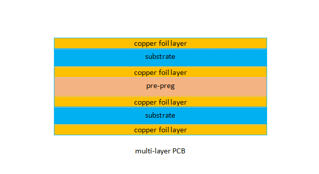
NC Drill – (Numeric Control drill machine) – A machine used to drill holes in printed boards at precise positions defined in a data file. A network is a group of terminals that are or must be electrically connected. Also referred to as signal.
Net – Also well as signal. A collection of terminals all of which are, or must be, connected electrically.
Netlist – A list of the names of symbols or pieces, as well as their logical connection points, in each net of a circuit. A netlist can be obtained from correctly prepared schematic-drawing files for an electrical CAE program.
Node - This is a pin or lead that is connected to at least one wire.
NPTH - NPTH are holes that do not have copper in the hole barrels are defined as NPTH’s.
Open – An unintended interruption in the continuity of an electrical circuit that prevents current from flowing.
Outer-Layer – The top and bottom surfaces of any circuit board.
Pad: This is one of the most basic components of a PCB assembly. A pad is a contact point that connects components to a via and serves as the soldering point for those components.
Panel – A material (often an epoxy-copper laminate known as FR-4) designed for the manufacturing of printed circuit boards.
Panelize: The process of grouping numerous PCBs into a panel to increase manufacturing efficiency.
Pattern – The arrangement of conductive and nonconductive materials on a panel or printed board. Also included are circuit configurations for relevant tools, drawings, and masters.
Pattern Plating – The selective plating of a conductive pattern.
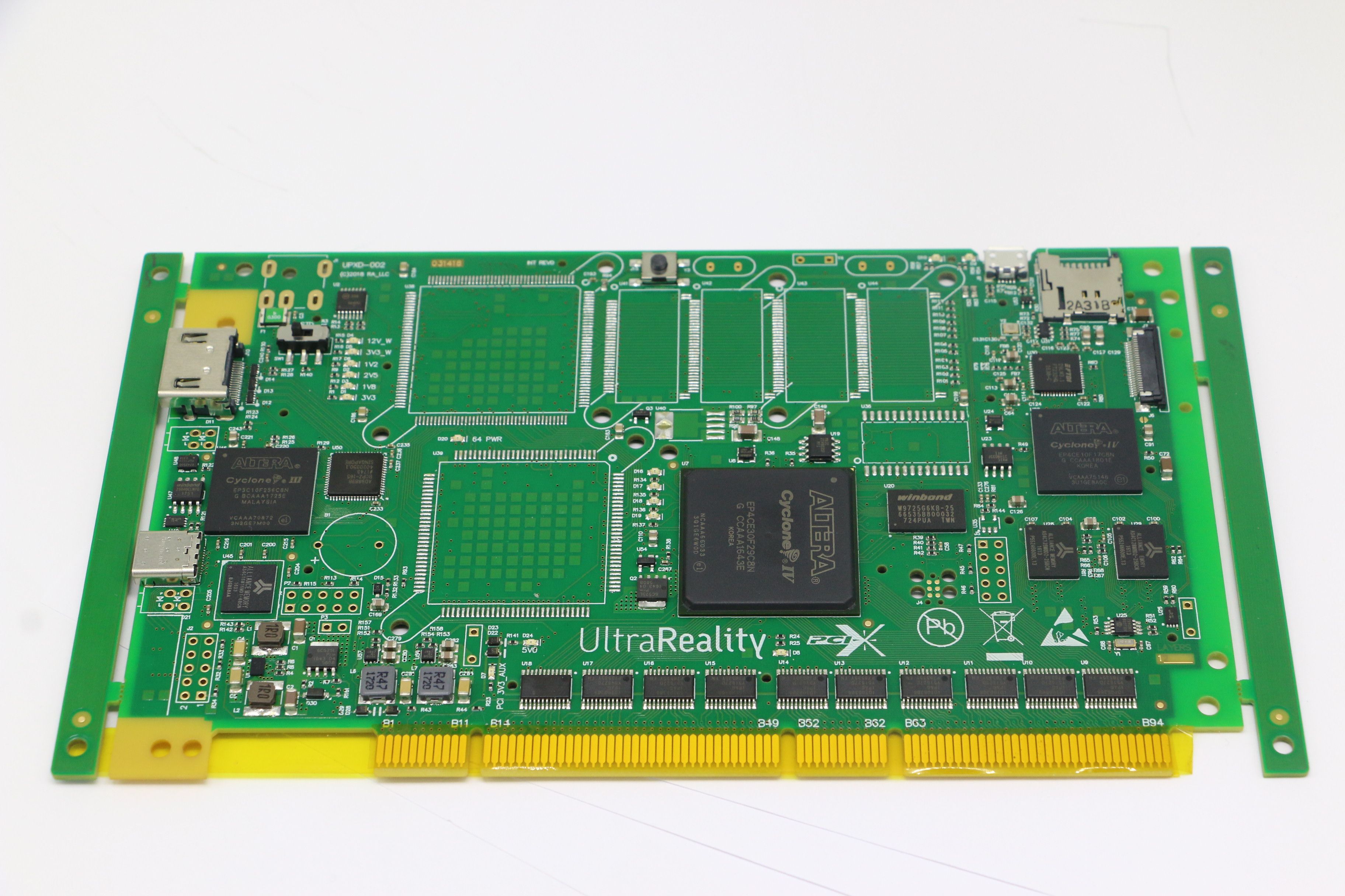
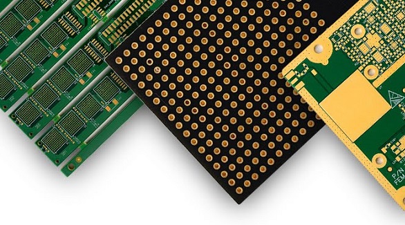
PCB - An abbreviation for Printed Circuit Board, a PCB is a board with conductive material and components that work together to generate a desired response. PCBs rely on electrical circuits that are printed or soldered onto the board to get the intended outcome. Printed circuit boards come in a wide range of shapes, sizes, and uses to fit any industry or application.
PCBA - Stands for Printed Circuit Board Assembly, which is when a manufacturer solders components to boards.
PCB Array - Boards supplied in pallet form, sometimes called "panelized", "stepped out", "palletized" and "rout and retain."
PCB Prototype - A printed circuit board prototype is one that is specifically made for testing purposes. An application may require a printed circuit board to be produced quickly in certain situations.
Photo Plotter – Device used to generate photographically by plotting objects onto film for use in manufacturing printed wiring.
Photo Resist – A material that may effectively hide high-integrity areas of a base metal by absorbing light in specific wavelength ranges.
Phototool – A clear film with the circuit pattern on it, shown as a high-resolution set of lines and dots.
Pin – A terminal on a component, whether SMT or through-hole.
Plating – Refers to the chemical or electrochemical deposition of metal on a surface.
Plated-Through Hole – A hole in a PCB with metal plating applied after drilling. Its function is to operate as either a contact point for a through-hole component or a via.
Positive – A developed image of a photo-plotted file in which the portions selectively exposed by the photo plotter are black and the unexposed areas are clear. Color will indicate copper in outer layers. Positive inner layers will have distinct copper-indicating regions.
Prepreg – A sheet of material that has been impregnated with resin and cured to an intermediate state. For example, B-stage resin.
Press Fit Holes: These are holes through which a contact terminal can be pressed into a PCB.
Printed Wiring: A procedure in which a design is etched into conductive metal on a board, resulting in a wire design for the PCB.
Probe Test – A spring-loaded metal item used to establish electrical contact between test equipment and the unit being tested.
Pulse Plating – A plating technique that uses pulses rather of direct current.
Reference Designator – The name of a component on a printed circuit that begins with one or two letters and ends with a numerical number. The letter denotes the component's class; for example, "Q" is a frequent prefix for transistors. On a circuit board, reference designators are typically represented by white or yellow epoxy ink (the "silkscreen"). They are positioned near their appropriate components, but not beneath them. So they are visible on the assembled board.
Reference Dimension – A dimension without a tolerance that is used solely for informational purposes and does not govern inspection or other production procedures.
Reflow – The process of melting electrodeposited tin/lead and solidifying it again. The surface looks and feels like it has been hot-dipped.
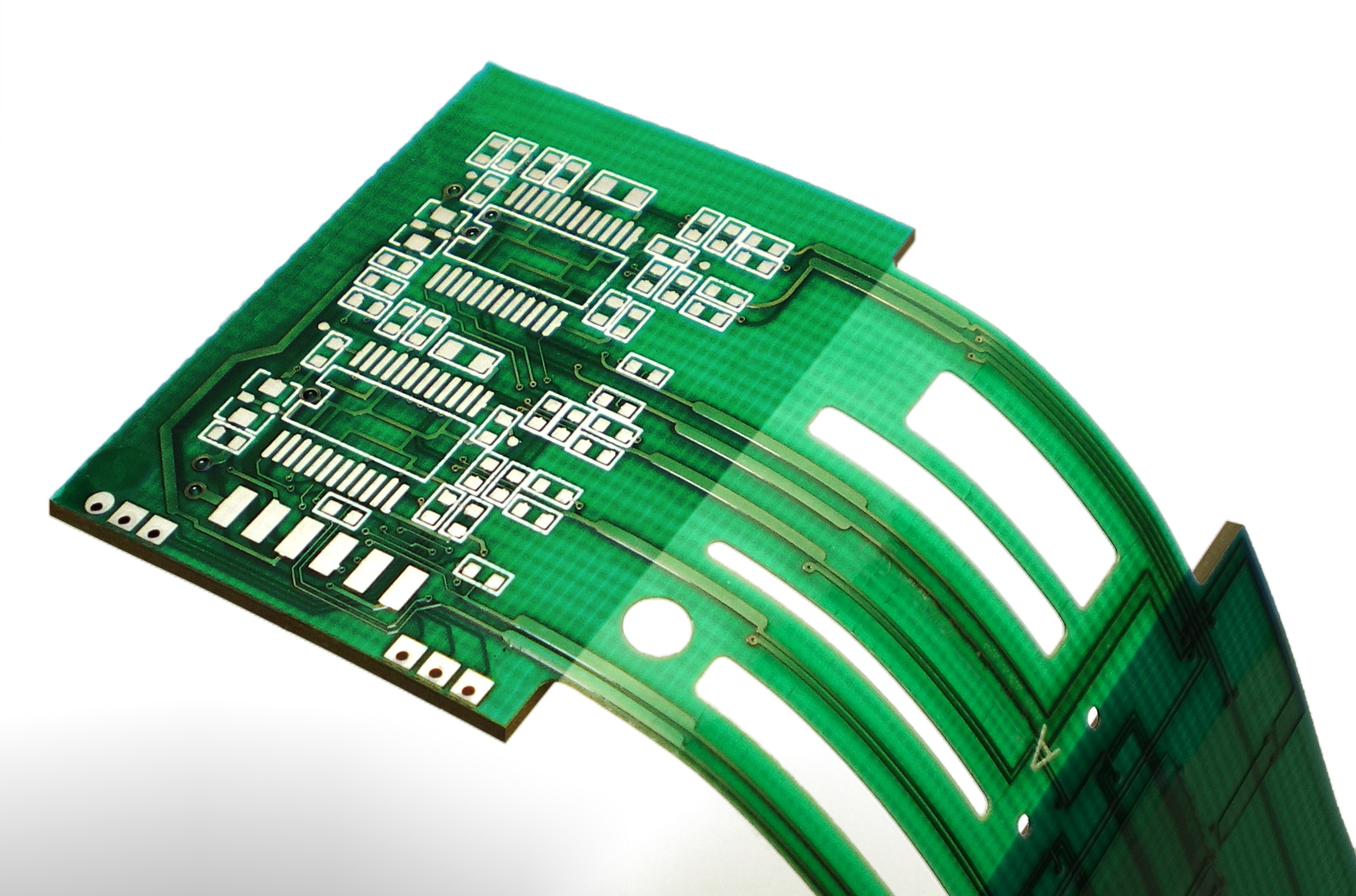
Rigid-Flex - Rigid-flex is a PCB structure that combines flexible circuitry and rigid multi-layers, typically to offer a built-in connection or to create a three-dimensional form with components.
RoHS – The RoHS Directive and similar legislative acts in other parts of the world are fostering changes in the fabrication and assembly of printed circuit boards.
Rough Holes - Rough holes have a copper burr around the entry or exit hole and lack a smooth barrel.
Rout – The layout or wiring of a connector. The process of establishing such a wiring. The term is also applied to the actual milling of a PCB.
Screen Printing – The method of transferring an image to a surface by pressing suitable medium through a stencil screen using a squeegee.
Short – An abnormally low-resistance connection between two circuit locations. The outcome is an excess (often harmful) current between these sites. A connection is regarded to have happened in a printed wiring CAD database or artwork whenever conductors from separate nets touch or get closer than the minimum spacing allowed for the design rules being applied.
Silkscreen –Decals and reference designators in epoxy ink on a printed circuit board, so named because the ink is "squeegeed" through a silk screen, the same technique used to print T-shirts. ACI requires a minimum line width of.008 for silkscreen.
Single-Layer PCB - A PCB design with traces and pads included on only one side of the board.

Slot Hole - Non-round holes on a PCB that may or may not be plated. These are often required for specific components but are costly due to the labor needed to cut them.
SMD (Surface mount device) - It refers to electrical components that are directly affixed to the surface of printed circuit boards (PCBs). Unlike through-hole components, which have leads put into holes on the PCB and soldered on the opposite side, SMDs are meant to be soldered directly onto the PCB's surface, making them better suited for automated assembly procedures.
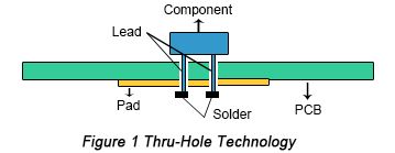
SMT (Surface Mount Technology) - A method of creating electronic circuits in which components are put or placed directly on the surface of printed circuit boards (PCBs). SMT has mainly superseded the old through-hole technology building approach, which involves inserting components with wire leads into holes in the circuit board.
Solder – An alloy that melts at relatively low temperatures and is used to join or seal metals with higher melting points.
Solder Coat – A layer of solder poured directly from a molten solder bath to a conductive design.
Spacing - This term refers to the distance between wires on a PCB.
Substrate - Another word for "PCB base material," which is the fundamental material used in PCB construction. This material can be flexible or rigid and composed of epoxy, metal, ceramic, or other materials. The purpose of the end PCB typically determines which substrate is utilized for the project.
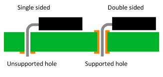
Supported Hole - This is a via having pads on both sides of the PCB. It is also plated within the via. This signifies that the entire hole is capable of supporting thermal or electrical conductivity tasks.
Surface Finish - Because copper oxidizes in natural surroundings, a surface finish prevents the layer from doing so. Oxidation might lead to tin paste failure or faulty soldering. Surface finishes include HASL, ENIG, IMAG, and OSP, among others.
Tented Via – A via with a dry film solder mask that completely covers both the pad and the plated-through hole. This totally isolates the via from outside objects, preventing unintentional shorts, but it also makes the via worthless as a test point. Vias are sometimes tented on the top side of the board and left uncovered on the bottom side to allow for probing solely from that side using a text fixture.
Test Board – a printed board that is thought to be appropriate for determining the acceptability of a collection of boards.
Test Fixture – A device that interfaces between test equipment and the unit under test.
TG – When temperatures rise, the resin inside the solid base laminate begins to develop soft, plastic-like symptoms. This is stated in degrees Celsius (°C).
Thou: This abbreviation stands for a thousandth of an inch.
Through-Hole – Pins that are designed to be put into holes and soldered to pads on a printed board. Also spelled "thru-hole"
Trace – A section of a conductor route or network.
UL – (Underwriter's Laboratories, Inc.) – A corporation formed by some underwriters to create safety standards for various types of equipment or components. The AC logo displays our UL certification.
Via – A plated-through hole on a printed wiring board is used to send a trace vertically through the board, from one layer to the next.
Void – The absence of all substances in a certain area. (Example: lacking plate in a hole)
V-Scoring - Rather than following a route path around the board edge, the edges are "scored" to allow boards to be separated after assembly.
Wave Soldering – Assembled printed boards are brought into contact with a continually flowing and circulating mass of solder, usually in a bath, to connect component leads to through hole pads and barrels.
Wire - A conductive cable capable of transmitting electricity or heat. It can also refer to a route or track on a printed circuit board.
Hot Tags:

Contact us

If you can't find what you're looking for, please contact us.
Article
One is a bare circuitry board, and another has all the components and is functional: PCB stands for Printed Circuit Board, and PCBA stands for Printed Circuit Board Assembly. PCB acts like a base, and components are assembled on it at a later stage through various methods in PCBA, such as SMT and Thru-Hole Technology.
 2024/07/29
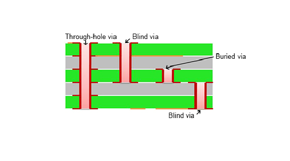
A printed circuit board includes a number of copper foil circuits, which are interlinked by vias. Via (through-hole, blind, buried, stacked, microvias) provides critical interlayer connections in high-density interconnection boards. Blind and buried vias increase the density of boards without adding size; hence, they are imperative for modern trends of miniaturization and high-speed signal transmission. These vias are plated with conductive materials, usually copper, so the electron flow can happen without much effort. Although advanced via types, like stacked vias, cost more, they save up much space and significantly improve routing capacity.
2024/07/26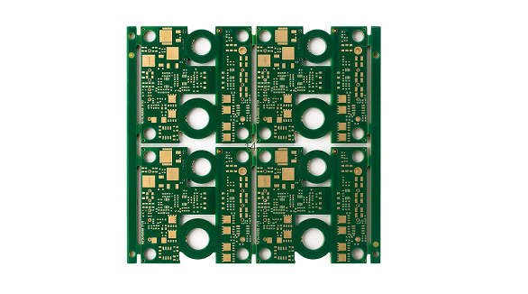
Most electronic circuits are mounted on PCBs, or Printed Circuit Boards, which provide mechanical support and electrical interconnection of electronic components. There are, however, special applications that involve the use of single and double-sided PCBs, multi-layer PCBs, or even rigid and flexible PCBs with aluminum backing, targeting medical, industrial, auto, and aerospace industries. They may use materials such as fiberglass, epoxy, aluminum, and others.
2024/07/25