QFP vs. QFN Packages
QFPs offer ease in inspection and modification with exposed leads, while QFNs provide compact design and superior thermal management, ideal for various applications.
Within this complicated world of electronic design, integrated circuit packaging fills an important part in deciding how components will connect and interface with other, much larger assemblies. Two such well-known alternatives for achieving that involve the Quad Flat Package and Quad Flat No-lead, with a particular application that shows its respective advantage over different needs. Here, we look into the characterizations, advantages, and basic differences that exist between QFP and QFN packages, giving some insights into their applications and assembly processes.
QFP Packages
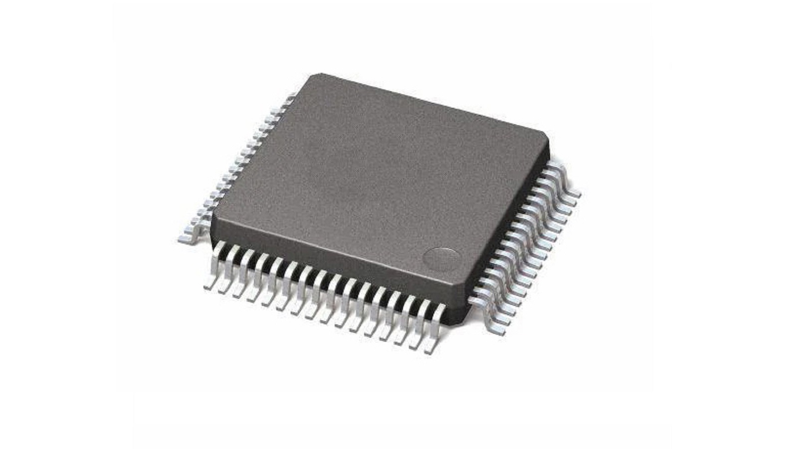
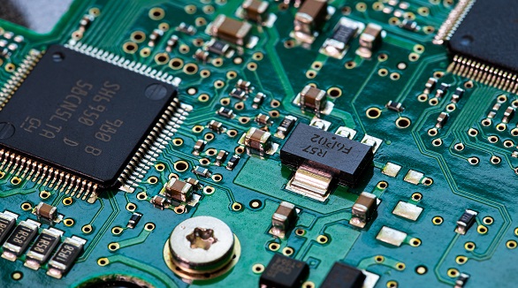
QFPs are one of the standard package types in IC packaging, with their typical "gull-wing" leads extending from all four sides. Packages of this type have been widely adopted due to their versatility and dependability regarding IC connections to printed circuit boards. Now, let's look into what makes QFP one of the favored choices:
Versatility and Ease of Inspection
The leads in QFPs are bent inward to allow a "gull-wing" shape, enabling robust surface mounting, easy inspection, and rework. The visibly accessible leads make them ideal for assembly and debugging in prototyping and development environments.
Applications
Because of the ability to support dozens of connections, QFPs find use in such applications as microcontrollers and microprocessors and highly complex digital or analog ICs. The package of choice for the simple reason that they support high pin counts.
Package Dimension and Construction
Made from plastic, there is also a square and a rectangular type QFP made from ceramic and metal. QFPs made from Plastic types are widely used since they are economic and widely accepted by all applications.
Variants of Packages
QFPs are available in many package variations, such as the BQFP, which has bumpers; a ceramic version; and a low-profile quad flat package, better known as the LQFP, used when profile height is a critical factor.
Assembly Advantages
Since the leads of the device are exposed, access to connections by soldering or visual is greatly enhanced, hence ease of repairs and modifications, particularly significant during development cycles.
QFN Packages
QFNs are a modern shift in the direction of efficiency and miniaturization. Following are the key characteristics that define these packages: compact design for high-performance applications, where space and thermal management are at a premium.
Compact and Efficient Design
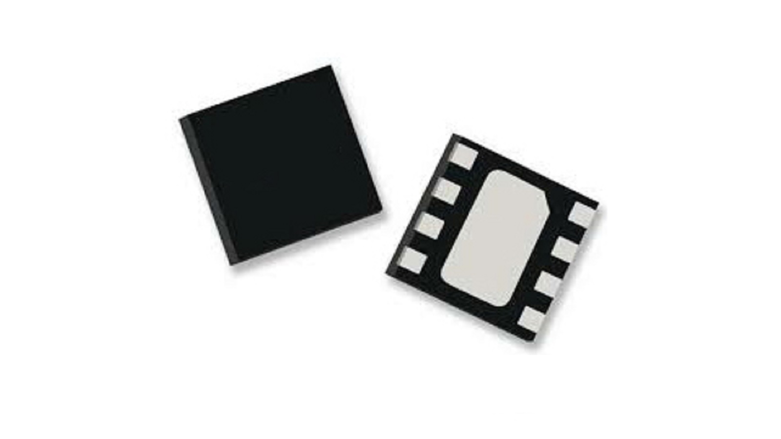
QFN has a pad at the bottom of the package rather than extended leads, giving a reduced footprint. This will maximize board space and help to move toward more compact and highly packed electronic assemblies.
Thermal and Electrical Performance
QFN packages are primarily characterized by offering excellent thermal performance. There is significant heat dissipation with the inclusion of a central thermal pad. Due to short electrical paths, parasitic inductance is reduced, thus ensuring signal integrity, which becomes quite useful in RF and high-frequency applications.
Types and Applications
The QFNs, which include Plastic-molded and Air-cavity types, address several GHz applications to very high frequencies. Since the form factor is the smallest, it will support high-density applications and also consumer electronics.
Manufacturing Process
QFNs fabrication involves saw singulation, punch singulation for getting multiple rows and pins amongst other techniques. One of the most important elements about the design is paying serious attention to the thermal pad, which needs to be designed well for good heat transfer efficiency.
Assembly Insights
The leadless design minimizes mechanical vulnerabilities, majorly requiring X-ray inspection and other advanced inspection techniques to verify solder joint integrity. This aspect might raise the initial production complexity; however, it leads to a compact product that results in higher performance for a compact product.
Differences Between QFP and QFN
Although QFP and QFN enable SMT, their differences need to be understood in relation to the selection of the right package for your application.
Lead Design and Connectivity
QFPs: Exposed leads extending outward simplify manual soldering and inspection processes, advantageous for environments where rework is common.
QFNs: Feature no outward leads, focusing instead on compactness and efficiency in board space utilization.
Size and Board Real Estate
QFPs: Demand more board space due to extending leads, which can be a limitation in space-constrained designs.
QFNs: Offer reduced footprints, allowing denser layout designs and more efficient utilization of PCB space.
Thermal Management
QFNs: Better at heat management because of the thermal pad at the center; thus, they become suited for applications with high needs of heat dissipation.
QFPs: Which may entail additional thermal management strategies.
Ease of Assembly and Inspection
QFPs: Offer unproblematic visual inspection and repair opportunities, increasing their value in prototyping and high-rework jobs.
QFNs: Depend upon automated inspection as the solder joints are invisible, and manual inspection is hard but offers several advantages in automated manufacturing systems.
Applications and Performance
QFPs: Applicable to complicated ICs with intensive I/O connectivity, QFPs find applications over a wide range where easy debugging is necessary.
QFNs: These are most applicable in high-performance and space-sensitive applications where either high frequency or intensive thermal load exists.
Assembly Considerations
QFP and QFN packages, for instance, need such an assembly process for their connections to be reliable in function:
QFP Assembly: Apply solder paste via stencil, place the component with accuracy, followed by controlled reflow soldering. Protect leads from mechanical damage during handling.
QFN Assembly: Emphasize accurate stencil design for solder paste application, ensuring a balance to avoid voids. Ensure precise placement of thermal pads and use controlled reflow soldering to secure the package.
QFP or QFN package selection depends on the specific demands of an application: space, thermal performance, or ease of assembly. Applications that require inspection ease and high pin counts prefer QFPs, while efficiency, thermal management, and compact design requirements are the niches for QFNs.
It helps the engineers to make a better judgment by weighing the various advantages and challenges of each package, thus coming out with improved performance, reliability, and compactness of the electronic product. Conclusion Both QFP and QFN packages are very important in shaping up the next generation of technological innovations as electronics continue to advance.
Hot Tags:
Contact us

If you can't find what you're looking for, please contact us.
Article
FPGAs offer high flexibility and capacity for complex designs, while CPLDs provide simplicity and cost-effectiveness for smaller applications, crucial in PCBs.
Routine inspections and proper maintenance of capacitors and resistors in PCBs reduce failures, prolong device lifespan, and lower maintenance costs.
SMT assembly streamlines electronics manufacturing with compact, reliable designs using precise equipment, meeting high-density demands and international standards.
