SMD Package
SMDs enhance compact, efficient PCB designs, streamline production, and boost performance in electronics by enabling high-density layouts and automated assembly.
With the fast-growing industry of electronics, the need for devices to be compact and efficient is always at an all-time high. The answer to these needs comes with SMDs, which allow high-density PCB designs not achievable by through-hole technology. The different package types for SMDs are necessary to understand in the interest of optimizing electronic designs and manufacturing processes.
The physical forms of SMT components are known as SMD packages, which allow them to be directly mounted onto the surface of a PCB. Unlike conventional through-hole components, which need lead insertion into drilled holes, SMDs make for space-saving, automated assembly, thus becoming ideal for high-volume and miniaturized electronics production.
Significance of SMD Packages
SMD packages differ according to the component type, size, and application; each has its advantages that relate to PCB design and manufacturing. The right choice can improve performance, facilitate production, and lower costs.
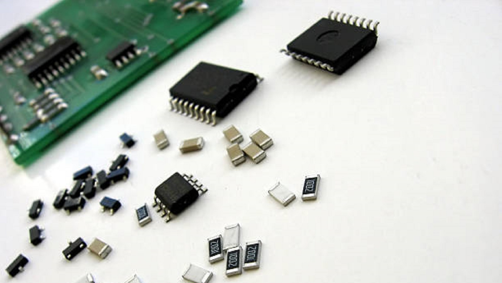
SMD Package Types
Discrete Surface Mount Resistors:
Thick Film Resistors: Employ a ruthenium dioxide-based paste screened onto alumina, providing inexpensive solutions for general applications.
Thin Film Resistors: Constructed on ceramic substrates with protective coatings, providing higher precision and stability, ideal for critical applications.
Resistor Networks:
R-Packs: Replace multiple resistors, optimizing board real estate and reducing placement time, crucial for densely packed PCBs.
Ceramic Capacitors for Surface Mount:
These capacitors play a very important role at high frequency and deliver dependability in small packages. They are used everywhere in decoupling and frequency regulating applications.
Leadless Ceramic Chip Carriers (LCCCs):
Featuring gold-plated castellation terminations, they reduce signal paths, allowing for higher operating frequencies.
Quad Flat Packages (QFP):
Standard QFP and Thin QFP (TQFP): Having leads on four sides, they are perfect for high pin-count, lower profile applications.
Plastic and Thin Plastic QFPs (PQFP/TQFP): Employed in VLSI circuits. TQFPs are powerful solutions for assemblies with difficult problems.
Integrated Circuit SMD Packages:
Small Outline Integrated Circuit (SOIC): Packages with gull-wing leads at 1.27 mm spacing support small form factor designs.
Variants include SOP, TSOP, SSOP, and TSSOP: Provide progressively narrower pin spacing to meet different density and profile requirements.
JEDEC Package Standards for SMT
The JEDEC standards allow for the compatibility and efficiency of SMT component sizes and configurations across industries. These standards make the work of designing PCBs easier with standard pad outlines, manufacturing processes more consistent, and assembly lines more automated.
Importance and Benefits of SMD Packages
Space Efficiency: Smaller packages allow more components per PCB, which is critical to making portable and compact devices.
Better Performance: Packages such as QFP and BGA address high-performance applications with advanced connectivity and thermal management.
Simplifying Manufacturing: Standardized package sizes allow streamlining of production, reducing costs and complexities.
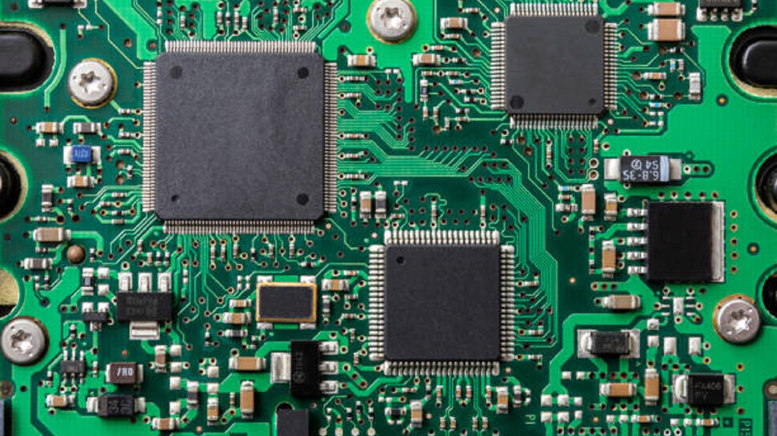
The very basis of modern electronics production is SMT and the different types of SMD packages. Understanding the characteristics and applications of each of these package types will allow the engineer to make appropriate choices that will enhance the design of a product and its manufacturing efficiency. As technology evolves, so does the evolution of SMD packages, driving innovation and performance in the electronics industry.
Hot Tags:
Contact us

If you can't find what you're looking for, please contact us.
Article
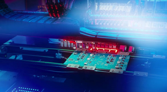
Surface Mount Technology revolutionizes electronics, offering size, cost, and performance benefits, but poses challenges with high setup costs and handling.
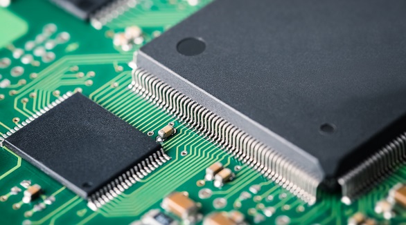
Surface Mount Technology (SMT) revolutionized electronics, facilitating smaller, faster, and more reliable products. It mounts components directly on PCBs, enabling miniaturization and automation. Though SMT boosts space efficiency, cost-effectiveness, and reliability, it poses rework challenges and requires high initial investment.
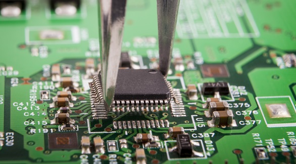
Still, SMT can further feature defects such as solder bridging, cold solder joints, tombstoning, and solder balling. Grasping the very common faults and their solutions is the key toward effective PCB assembly and reducing SMT errors—very much in line with the trend toward PCB miniaturization and higher component density.