SMD vs. NSMD
SMD offers stability and control in PCBs, ideal for high-density uses. NSMD provides flexibility and stronger joints, better for mechanical tolerance.
Decisions related to pad style-a Solder Mask Defined vs a Non-Solder Mask Defined-can greatly impact assembly processes, mechanical reliability, and functional performance in the field of PCB design, especially when using Ball Grid Array packages. This paper represents a deep, professional comparison of SMD and NSMD pads with their respective pros and cons, considering their application in diverse scenarios.
SMD and NSMD Pads
The definition of a pad in PCB design deals with the relationship of the solder mask to the copper pad.These copper pads are critical components of PCB design for forming strong, durable solder junctions. In these pad specifications, both primary kinds, SMD and NSMD, have features that make them suitable for varied applications.
What is an SMD (Solder Mask Defined) Pad?
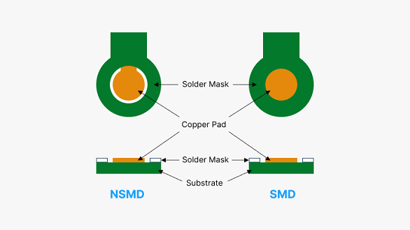
SMD pads are defined by having their edges covered by the solder mask. The solder mask opening is narrower than the actual copper pad, which defines the pad's effective dimensional boundary.
Advantages
Improved Mechanical Stability: This overlap in the solder mask provides better mechanical support for resistance against thermal cycling and other forms of pad lifting.
Solder Volume Control: SMD pads provide a means for better control of solder paste volume, which would reduce the risk of solder spattering and bridging upon reflow.
Precision in High-Density Applications: They are ideal for applications requiring high density and precision since they keep the profile neat and clean in a connection.
Disadvantages
Limited Pad Size: The exposed copper pad to air is smaller, which may lead to reduced solder joint strength.
The Risk of Solder junction Cracking: Due to mask thickness, the pad has less flexibility; hence, it may cause the junction to shatter once pressured.

What is an NSMD Pad?
The solder mask opening in NSMD pads is larger than that of the copper pad size. Hence, all the copper surface is free.
Advantages
Increased Pad Flexibility: The pad, which has not suffered the restraint imposed on it by the solder mask, is capable of flexing without such risk of solder joint cracking.
Larger Solderable Surface: Thus, the solder has been allowed to adhere to the top and the sides of the pad, increasing the reliability of the joint through greater resistance against mechanical stress.
Improved Design Flexibility: NSMD pads, moreover, offer greater flexibility in design from the standpoint of shape and size, which may be optimized for specific application needs.
Disadvantages
Limited Solder Volume Control: Without mask limitations, volumes might fluctuate, resulting in bridging.
Higher Cost of manufacturing: The precision required for mask and pad alignment may raise manufacturing costs.
SMD vs. NSMD Key Differences
Pad Design and Configuration: In SMD, the solder mask is used to define the pad dimensions. The NSMD pad has entirely exposed copper, however. This allows for a lot of flexibility and personalization.
Mechanical Stress Tolerance: Due to mask overlap, the SMD pad is much stronger mechanically. While NSMD presents a design that, due to mechanical stress distribution, can bear greater levels of it.
Flexibility of Pad Design: NSMD pads allow the flexibility of pad shape and size to accommodate various custom designs, which is highly useful in applications like BGAs where adaptability is so crucial.
Compatibility for High-Density Uses: SMD pads are best suited for tight-pitch and high-component density applications because of controlled reliability with least possibility for solder bridging.
Implications of the Soldering Process: This decision has a significant influence on soldering applications. SMD pads restrict solder volume, but NSMD pads, while flexible, require vigilance to avoid issues.
Conclusion
The final selection between SMD and NSMD pads is determined based on the unique PCB design requirements and the application environment. SMD pads are actually designed for precise and controlled processes, perfect for intricate, high-density configurations that require good mechanical stability. NSMD pads, however, are better in terms of creating design flexibility and stronger solder joint formations; thus, they can be applied in cases requiring high mechanical tolerance and reliability.
These differences, when well understood, help the PCB designer make relevant choices to achieve the best performance, cost, and reliability in a variety of electronic applications. To this end, the correct selection of pad type becomes an integral part of any successful execution of a PCB project to ensure feasibility for current manufacturing standards and demands of the intended application.
Hot Tags:
Contact us

If you can't find what you're looking for, please contact us.
Article

The article provides a step-by-step guide to soldering a PCB, covering workspace setup, essential tools, and safety measures. It explains heating the soldering iron, applying flux, tinning the iron tip, placing components, heating joints, applying solder, cooling, inspecting, and cleaning. Emphasis is on practice and safety for successful soldering.

Solder masks protect PCBs from environmental damage and electrical shorts, enhancing reliability and aesthetics. The application is complex, requiring professional fabrication to ensure quality and compliance with regulations.

The article explains the current situation of Printed Circuit Boards and future development based on efficient production helped by advanced software and manufacturing processes. Future technological developments are in store for 3D Printed Electronics, flexible PCBs, eco-friendly biodegradable PCBs, and board cameras. It elaborates on other powerful automation tools that are going to make the entire PCB design process efficient in the near future. All of them will further improve and develop with the technological advances in PCBs, keeping up with the ever-increasing industry and consumer demands.