- Products & Capabilities

- About
- Resources
Single-Layer vs.Multi-layer PCB


Choose between single-layer or multi-layer PCBs based on your project's needs. Single-layer is simpler and cost-effective; multi-layer offers complex functionality and durability. Evaluate based on functionality, size, durability, budget, and turnaround time.
Before designing a printed circuit board (PCB), you must decide whether to use a single-layer or multi-layer PCB. Both will be evident in a variety of common gadgets, but the optimal option will be determined by the unique needs of your project. In general, more advanced devices use multi-layer boards, while simpler devices can benefit from single-layer boards. This article aims to point out the key differences between these choices, to help you select the right type for your project.
Single-Layer vs. Multi-Layer PCB: Key Differences
The number of layers is the primary distinction, as the names imply, between a single-layer and multi-layer PCB. A single-layer PCB contains only one layer of base material (the substrate), whereas a multi-layer PCB has numerous layers. Moreover, a little closer inspection reveals more differences in their construction and functionality.
Single-Layer PCB

In other words, single-layer boards are single-sided PCB with components mounted on one side and a conductor pattern on the other side. Single-sided PCB contains only one layer of conductive material, commonly made of copper. A single-layer board commonly comprises a substrate layer, a conductive metal layer, a protective solder mask, and a silkscreen layer. Single-sided PCB is mostly applied to simple electronic gadgets.
Double-Layer PCB

Double-sided or double-layer boards have more than one layer, although less than multi-layer boards. A double-sided PCB will have the same single substrate layer, but there will be a layer of conductive metal, the circuitry layer, on both sides of the substrate. Generally speaking, circuits on one side of the board will connect with circuits on the other side of the board using either a through-hole or a surface-mount method :
- Through-Holes: Small holes are drilled through the board to allow leads (wires) to be laid and soldered to the right component.
- Surface Mounts: Leads are soldered straight on the board, making the board the wiring surface in and of itself. This design approach is advantageous because it allows relatively compact circuits to work.
- Multi-Layer PCB
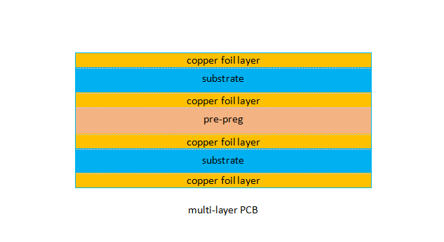
- Multi-layered PCBs are stack-ups in several more than three double-sided boards. They theoretically can contain any number of layers, but the most a PCB was ever produced with was 129. They usually include an even number of layers — four to twelve — as odd numbers complicate problems with warping and twisting after soldering.
- Each layer in a multi-layer board has conductive material coated on both sides. These substrates are adhered together using a special adhesive, and an insulating material is used to separate the boards. On the external sides of the multi-layer board are solder masks.
- Vias are certain pathways that connect and conduct to the other different layers. These different kinds of pathways can be of three types:
- Through-Hole Vias: These are channels that reach into every board layer.
- Buried Vias: This type of via connects one inner layer to another, so it cannot be seen outside.
- Blind Vias: These serve as a link between an inner and an outside layer.
- These kinds of PCB are generally made for usage in more complex devices since the number of connections is much higher in them.
Advantages of Single-Layer PCB
There are a few strong reasons to employ single-layer PCB in your project, based on your needs. The major advantages of single-layer PCB are as follows.
- Lower Cost: Single-layer PCB is easy to design and fabricate in comparison with double or multi-layer PCB. Single-layer boards require less material, less time, and few skills; hence, they are more cost-effective. Generally, the single-layer PCB would be much more economical if the job specifications can be achieved without sacrificing quality and performance. Its lower cost is a major advantage when compared with multi-layer PCB.
- Simpler Design and Production: The simple nature of single-layer boards allows them to be designed and produced easily and be put into almost any design, so it is popular among designers and manufacturers. It has resulted in a less cumbersome and more consistent production process than that for multi-layer PCB.
- High-volume production: Single-layer PCBs are simple to manufacture and require little effort in total. When a large quantity is ordered, the cost decrease per board is minor, but the above costs add up to a high profit.
- Short Lead Time: Due to their simple design and fewer resource requirements, single-layer boards can be produced fast and easily, which makes them the ideal option for projects where a faster turnaround is needed, even in huge quantities.
Disadvantages of Single-Layer PCB
- Simple Design: Where simplicity is an advantage, it also limits the functionality of single-layer boards. Complex devices requiring several components and connections may not have enough space or power in a single layer. If wires cross, the device may not work properly. Adequate space and a proper layout, therefore, are a must. Simply, a more sophisticated design cannot be accommodated into a single-layer PCB.
- Slower Speed and Lower Operation Capacity: Limited connections reduce power and slow the speed for single-layer PCB. Lower-density designs decrease the ability to transmit the same power and maintain the same speed, which might impact many applications, requiring the higher robustness and operating capacity of multi-layer PCB.
- Larger Size and Higher Weight: Any addition of functionalities in a single-sided PCB always requires an increase in size. However, the dimensions become large quadrilaterally, thus requiring more space compared to a multi-layer PCB. This may lead to adding more layers. The possibility of using multiple separated boards is always there, but a single multi-layered board can handle the requirements. Moreover, an increase in size or number of boards would mean an increase in the weight of the device, and this can, in some cases, affect the final product for which it is intended.
Pros and Cons of Single-Layer PCB
After evaluating the requirements of your project, you must confirm if a single-layered PCB is up to your needs. Single-layered PCB is usually applied to basic gadgets because they are low-priced and have preeminent advantages like faster production than counterpart boards. However, it is not the best choice for more integrated projects.
The pros and cons can be summarized into:
Pros:
- Low cost
- Simple design and production
- High-volume production capacity
- Shorter lead time
Cons:
- Too simple for complex projects
- Lower operation capacity
- Slower speed
- Larger size
- Heavy
- Summary:
- If the above features meet the criteria of your project, and the pros outweigh any cons, then single-sided PCB is nearly a good choice.
Single-Layer PCB Applications
Single-layer PCB is widely used in many applications due to its cost-effectiveness and ease of production. With the rising demand for multi-layer boards corresponding with the rising complexity of most electronic devices, the single-layer board is still the most common. Single-layer boards make a special niche for those devices accomplishing only one particular task and are not necessarily in need of storing voluminous data or internet connections.
Some common examples of single-sided PCBs include small appliances, such as coffee makers. Inside calculators, radios, printers, and LED lights are other typical applications. Single-sided PCB is also often used to build less sophisticated storage solutions like solid-state drives, power supplies, and a variety of sensors.
Advantages of Multi-Layer PCB
While single-class boards can carry advantages over multi-layered designs, the latter tend to be more beneficial for specialized functions. Multiple layers are even fundamentally necessary for some devices. The following are the advantages of multi-layer PCB:
- Useful for Sophisticated Projects: Multi-Layer PCBs can accommodate more circuits and elements. More layers provide the necessary area to connect components, allowing them to fit into these advanced devices, like smartphones.
- High Quality: Multi-layer boards are more intense in processes of planning and production; therefore, to ensure the quality of products. Advanced features such as controlled impedance and electromagnetic interference enhance product performance further.
- Added Power: Multilayer PCB has high circuit densities, hence they provide high operating capacities and are more powerful. They can run at higher speeds, which are necessary for advanced devices and, thus, promote better performance.
- Extra Strength: The extra layers found in multi-layer boards make them thicker and hence stronger than the single-sided boards. They are capable of withstanding harsher conditions and generally have a long life.
- Smaller Size and Lighter Weight: Multi-layered PCB provides reliability while keeping the size smaller and the weight lower. Stacking up the layers allows more functionality within a small space compared to single-layered boards, thus reducing the overall size and weight of the product.
- Single Connection Point: Having a single connection point in multi-layer boards helps design the electronic device more simply, and hence it further reduces the weight of the electronic device. Multilayer PCB is the better option because multiple single-layer boards require multiple connection points.
Disadvantages of Multi-Layer PCB
The advanced functionality and other benefits of multi-layer PCB come at a cost, which makes them might not be suitable for every project. Disadvantages are given below:
- Higher Costs: Because of the need for substantial resources, time, and skills, the design and manufacturing cost of a multi-layer board is higher than a single or double-layer one. No matter which kind of PCB, you must ensure that the benefits outweigh the costs.
- More Precise Design and Production: Multi-layered boards need more detailed design and production - hence it requests that designers and production engineers be very skillful. Also, the equipment used must be very specialized. From this view, its production may be very unwieldy if what is available is not what is needed.
- Less Availability: Multi-layer boards require specialization for their manufacture and hence not all vendors will be able to cater for this. It is not easy to get a reliable company to design, manufacture, or repair the printed circuit board.
- Longer Lead Times: The production of multi-layer board mainly needs a longer period, since making it secure is complicated, which adds up to the length of lead times. Rectification of designs or mistakes in production will also come with an increase in both lead time and possible expense.
- Complex Maintanace: Internal layering that would make it difficult to detect problems. Therefore, due to the elaborate structure, it is possible to have a higher count of the components thus taking up more time while repairing.
Pros and Cons of Multi-Layer PCB
Is multi-layer PCB suitable for your project? For intricate devices, they are probably the best choice for adding more functionality. But it is noticeable that this may come at a price. The pros and cons of the multi-layer PCB work toward your resource availability and the requirements of your project.
Pros:
- Complex functionality
- Quality
- More power, operational capacity, and speed
- Durability
- Small size and lighter compared to other alternatives
- Single-point connection
Cons:
- High cost
- Difficult to design and make
- Supply is not that large
- Lead times can be long and difficult to repair
Multi-Layer PCB Applications
With the advancement of the era, multi-layer printed circuit board (PCB) have become more popular. Most of the modern electronic devices have specific complex functions, which require the smaller the PCB, the more the number of layers. The applications for multi-layered PCBs are almost endless, ranging from devices that need to perform multiple functions to equipment with a specified complexity.
Computer Parts: Many computer parts, from motherboards and servers to computerized devices like laptops, tablets, smartphones, and smartwatches, are the basic corpus of multi-layer PCBs. For instance, there are generally 12 layers for smartphones. The systems that let electronics, like smartphones and laptops and other gadgets, with GPS capability work, from the phone towers to satellite technologies, also can't function without multi-layer boards due to the extremity in features.
Consumer Electronics: Appliances are generally more sophisticated than basic household devices, but less so than smartphones and signal devices, using PCB with 4-8 layers. Like microwaves and air conditioners, they are always increasingly produced with multi-layer technologies to increase their native capabilities.
Medical Devices: A good number of medical equipment are built on PCBs with more than three layers out of a need for reliability, compactness, and lightweight design. Like X-ray machines, heart monitors, and CAT scan machines, they all need multilayer PCBs.
Automotive and Aerospace Industries: The automotive and aerospace industries have become more electronics-friendly, so they demand the right balance of robustness and lightness. All these characteristics, among others, can only be performed by multi-layer PCBs. These components must be worn and high-temperature tolerable as well as severe conditions enduring. Multi-layered PCBs can be embedded in onboard brains, GPS systems, engine sensors, and headlight switches, among others.
Industrial Applications: The need for industrial multi-layered PCBs is increasing day by day. Modern industrial machines often comprise computerized controls and sensors working with intense levels of PCB. These machines not only require miniaturized design, but provide long-term reliability and service, and achieve considerable durability in the often wet and harsh conditions.
Other Usage: Besides the above areas, multi-layer PCBs are highly essential for the military, weather analysis equipment, alarm systems, atomic accelerators, or any other textual form of electronic equipment, owing to their unusual ability.
Multi-layer PCB therefore plays a central, indispensable role in enabling modern technologies to contain immense use, all with a need for complex functionality, reliability, and compact design. Its importance lies in enabling many electronic devices characteristic of modern everyday life.
Choosing Single-Layer or Multi-Layer PCB
The decision to utilize a single- or multi-layer PCB is based on the requirements of your project. The following five essential questions may help you make a choice:
- What level of functionality do I need?
- If a project requires a high level of capability, then multiple layers might be required.
- What is the maximum size for the board?
- Multi-layer boards can fit more functionality into less space; thus, making them ideal for design in tight spaces.
- Is durability a top priority?
- Multi-layer boards have increased durability, therefore, they are the better option when strength is critical.
- What is my budget?
- Single-layer boards cost less. They should be used for needs requiring modest budgets.
- How soon do I need PCBs?
- Compared with multi-layer PCB, single-layer one needs a shorter lead time to facilitate the accomplishment of your project.
- With this comes additional technical requirements for operating frequency, density, and the number of signal layers necessary. Knowing how your design will fit these standards can help you decide if you need a single-layer, double-layer, or multi-layer PCB. For further information, please see our resources on design considerations.
PCB Solution from PCBX
PCBX has the expertise, resources, and skill to deliver the best PCB solution for your project, whether you need single-sided, double-sided, or multi-layer boards. Whichever one you choose, we will provide high-quality components to you from reputable suppliers.
From fully featured production to complex assembly, we can meet all your needs, including the customized assembly of PCB and functional test by your unique specifications.
Contact us after completing our online form or by phone or email. Our staff members at customer service could give you support at all phases. Quote here: To learn more about our capabilities, you can go through the free resources (from standard PCB to layer stacking) available on our website.
Hot Tags:

Contact us

If you can't find what you're looking for, please contact us.
Article
Mounting holes in PCBs ensure mechanical stability, electrical functionality, and thermal management, crucial for design integrity and performance.
 2024/11/05
FR4 is a favored PCB material for its cost-effectiveness and versatility. However, its thickness tolerance impacts mechanical strength, thermal performance, and electrical efficiency, affecting overall PCB reliability and performance.
2024/09/24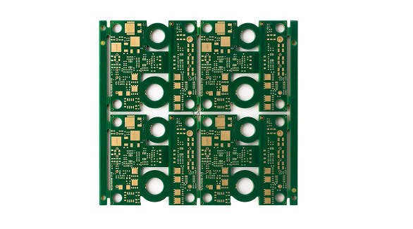
Most electronic circuits are mounted on PCBs, or Printed Circuit Boards, which provide mechanical support and electrical interconnection of electronic components. There are, however, special applications that involve the use of single and double-sided PCBs, multi-layer PCBs, or even rigid and flexible PCBs with aluminum backing, targeting medical, industrial, auto, and aerospace industries. They may use materials such as fiberglass, epoxy, aluminum, and others.
2024/07/25