Solder Paste Stencils in PCB Assembly
Solder paste stencils are crucial for accurate PCB assembly, offering precision and reduced defects. Various types, including laser-cut and hybrid, enhance manufacturing efficiency and product reliability.
In the complex world of electronics manufacturing, solder paste stencils are a cornerstone in the assembly process for printed circuit boards, more commonly referred to by their acronym as PCBs. This component, largely overshadowed by more visible elements, happens to play a very critical role in terms of the accuracy and functionality of electronic devices. At PCBX, we appreciate the intricate processes involved in assembling a PCB, the solder paste stencil being one piece that epitomizes a mix of precision and functionality. To that effect, this well-illuminated discussion explains what solder paste stencils are, the main benefits, types, components, and specifications they should have to ensure successful PCB assembly.
What is a Solder Paste Stencil?
The solder paste stencil is not just any tool; it is actually one of the more precisely conducted pieces within the process of manufacturing PCBs that use a thin sheet made from stainless steel, though other materials like nickel or polymer could well be used for such purposes. The stencil is characterized by a series of precisely laser-cut apertures mirroring the layout of the PCB's pads. These apertures allow the accurate deposition of solder paste onto the PCB at the time of manufacturing, preparing it for surface-mounted component placements. Since a stencil allows every aperture to perfectly match up with its respective pad on the PCB, it ensures maximum mechanical strength and electrical connectivity for the proper functionality of an electronic device.
Core Functions and Importance
The primary job of a solder paste stencil is to apply solder paste on the PCB in predetermined patterns where there are parts to be joined with solder. Paste, consisting of solder particles and flux, is applied via a squeegee, which evenly spreads the paste across the stencil. The paste fills the apertures, insuring just the right amount of paste is deposited onto each pad on the PCB. This process aids in correctly placing the component and soldering it securely during subsequent reflow processes.
Stencils for solder paste, from an operational standpoint, would like to facilitate the manufacturing process by encouraging one solid, reproducible technique for solder paste application. The rapid, accurate application with the stencils contributes to the reduction of human error and improves the quality of solder joint and component positioning, necessary for defect reduction and productivity.
Solder paste stencils, especially SMD stencils, boast a number of advantages that have become so vital in today's modern electronic manufacturing processes, to wit:
Uniform Solder Application: Perhaps the biggest advantage of applying a stencil is the ability to achieve even solder paste across the SMT pads. Uniformity in solder application reduces variability in solder joint quality and leads to consistent electrical connection, which is basic to device reliability.
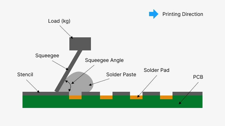
High Precision and Accuracy: SMD stencils offer high pad placement accuracy, which again translates to high precision of placing components. This has again become imperative not only for functionality but also in maintaining integrity with miniature and fine-pitch components of contemporary designs.
Reduced Manufacturing Time: Automating the application of paste is another means by which stencils help reduce time spent aligning components manually, hence reducing assembling cycles, thereby boosting the whole manufacturing process greatly or sometimes even being cost-effective with minimum runs.
Improved Quality of Solder Joints: With stencils, the distribution of solder paste will be even and controlled, which will raise the quality of the solder joint and thus lower the likelihood of defects such as bridging or voids normally affecting device dependability.
Lower Defect Rates: The precision of the stencils greatly reduces production defects, minimizing the potential for problems with component misalignment or less-than-optimal solder distribution. This in turn means fewer defects, which directly hits the bottom line by reducing costs associated with rework or trashed boards.
Types of PCB Stencils
The correct selection of the type of stencils is important as per specified requirements of manufacturing and to provide accuracy at assembly. Here, some of the common types of stencils available in the market are described below:
Laser-cut Stencils
These would be prepared by advanced methods of laser cutting, allowing precision in aperture size and shape. These would be more applicable to small pad sizes, fine-pitch components, or other applications where higher geometrical complexities are expected. Laser-cut stencils provide even higher accuracy and durability, hence very ideal for high-volume automated productions.
Chemical-etch Stencils
These are generally inexpensive and can be produced somewhat more quickly, using acid-based etching substances to burn apertures into metal sheets. On the other side of the coin is its environmental impact and precision-sometimes not up to par with laser-cutting equivalencies in terms of finesse.
Framed PCB Stencils
Framed stencils are widely used in volume printed circuit board fabrication. These are stretched on a frame or mesh border. It helps the stencil to stay taut for repetitive solder paste application. The tension from one use to another guarantees accuracy and quality of print.
Frameless/Reusable PCB Stencils
Frameless stencils are cost-effective, flexible, and suitable for small batch or prototype jobs. They require handling with care to maintain their accuracy but are adaptable for various board sizes and save storage space compared to framed types.
Prototype PCB or Photo Stencils
These are stencils made by the customer's specification from CAD or Gerber files. These are processed by photolithography and are very useful during prototype development, where a designer can refine the PCB design before scaling up into production quantities.
Hybrid PCB Stencils
These stencils use a combination of both chemical etching and laser cutting. It allows for high accuracy in intricate designs, supporting detailed customizations, longevity, and quality in repetitive use.
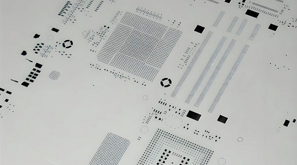
Structure of Solder Paste Stencil
The solder paste stencil involves a few key components:
Stencil Holder: Stencils could be held in movable or fixed holders. Movable holders secure the stencil around an reusable framework. Fixed holders are secured by adhesive that maintains uniform tension on the stencil.
Mesh: This is fabricated from either stainless steel or polymer polyester. It helps to attach the steel sheet to the holder. Stainless steel, even though providing stability, usually loses its tension after a while; whereas polyester brings the difference in terms of offering lasting strength without deforming.
Steel Sheet: Most stencils are made with the use of stainless steel sheets, as they can provide suitable mechanical properties, aside from copper and nickel alloys. These sheets normally play a very vital role in achieving perfect paste application.
Adhesive: It is chosen according to needs, adhesive applied for the mesh and stencil shall be in such a way that it provides high steadfast adhesion. This is also compatible with cleaning agents for the stencil.
Basic Requirements for PCB Stencils
There are some general requirements for a solder paste stencil to ensure proper and repeatable SMT application:
The reasons are:
Accurate Aperture Size and Shape: Apertures need to exactly match dimensions with the component pad for the correct application of paste volume. Normally, apertures are 5-10% larger than the pad to ensure coverage.
Exact Aperture Placement: The aperture placement accuracy is very important; normally, +/- 0.025mm or better is expected. This is to ensure the correct solder volume on each pad.
Adequate Thickness: Which offers proper balance between structural integrity and effective paste transfer. Standard thicknesses used range from 0.1mm to 0.2mm, often settling at 0.127mm (5 mils).
Consistent Aperture Walls: Should be free of burrs or defects and have a thickness tolerance in the region of +/- 0.0127mm.
Positioning of Fiducial marks: Alignment of the marks should be near to the PCB pads within the diameter of 1mm for accurate assemblies.
Compatibility: The design needs to be compatible with the machine intended for component placement and solder reflow so that smooth integration into the assembly line is guaranteed.
Conclusion
The stencil for solder paste plays a very important role in intelligent and reliable PCB manufacturing. At PCBX, we believe in precision and diligence in the application of these stencils to ensure that the resulting products are nothing short of exemplary. Appreciation of the different types of stencils, their structural components, and baseline requirements enables a manufacturer to have considerable leverage in the assembly process for efficiencies, low defect rates, and general quality improvement. For either rapid prototyping or volume production, the right solder paste stencil will meet functionality requirements and elevate the entire manufacturing process to a new height, making ways for innovation and excellence in the field of electronics.
Hot Tags:
Contact us

If you can't find what you're looking for, please contact us.
Article
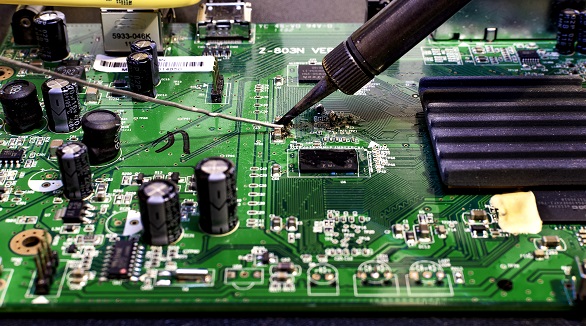
SMD soldering mounts small components on the PCB surface for compact, automated designs but has high setup costs and repair challenges. DIP soldering uses through-hole components for robust, easily repairable, lower-volume applications.
Wave soldering is vital for assembling printed circuit boards (PCBs), aiming to bond electrical components. The process involves passing PCBs over a wave of molten solder to form connections. Common defects include pin/blow holes, solder shorts, poor hole fill, lifted components, excessive solder, solder balling, and solder flags. To address these issues, key factors include proper flux application, controlled preheat temperatures, optimal solder wave settings, and careful material handling. Understanding and managing these factors ensures high-quality, reliable PCB assemblies.
Solder masks protect PCBs from environmental damage and electrical shorts, enhancing reliability and aesthetics. The application is complex, requiring professional fabrication to ensure quality and compliance with regulations.