- Products & Capabilities

- About
- Resources
Standard PCB Panel Dimensions


PCBs are essential for electronic devices, providing mechanical support and electrical connections. This article explores the importance of PCB panel dimensions, standard sizes, and optimization techniques. Key points include cost-efficiency, ease of manufacturing, quality control, and optimal layouts. Factors like board size, volume needs, and equipment capabilities influence panel size. Coordination with manufacturers, using design software, and employing standard sizes can enhance production efficiency and quality.
Printed Circuit Boards (PCBs) make up the backbone of any modern electronic device. Many intricate processes and decisions have to be made in designing and manufacturing a PCB, which greatly impacts cost, performance, and production efficiency. The dimension of the PCB panel is very critical in all these. This article will explain standard PCB panel dimensions, their importance, and how to optimize them according to your need.
What Are PCBs?
PCBs are meant for providing mechanical support and the electrical connection with the help of conductive pathways/tracks/signal traces that are etched from copper sheets afterward and laminated onto the non-conductive substrate. It turns out that these components and connections can have a single-layer, double-layer, or multi-layer format.
What is an array PCB?
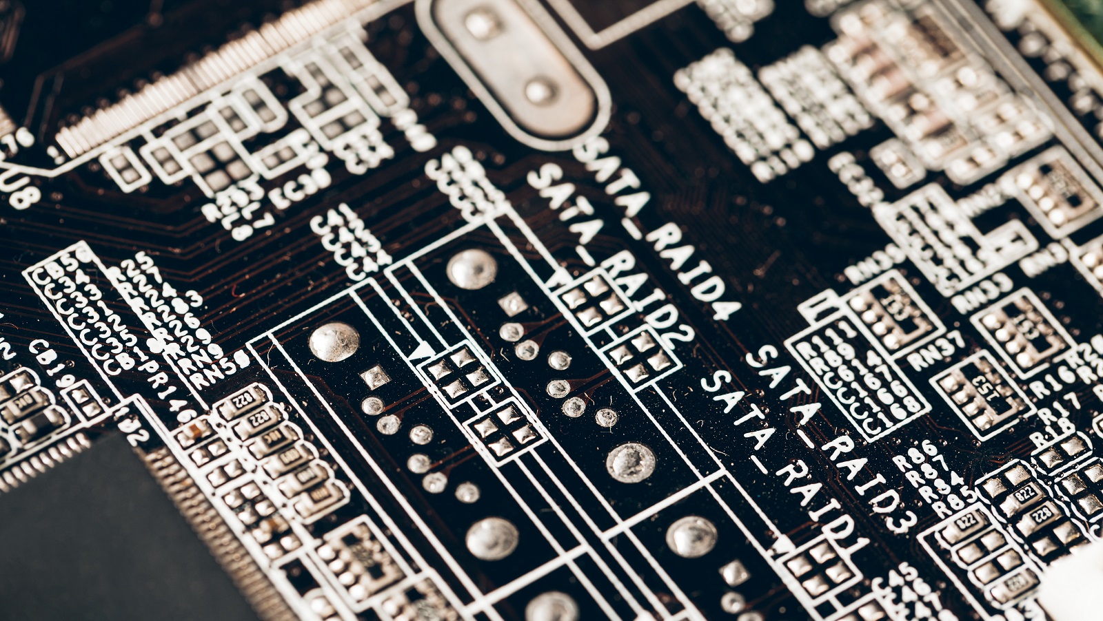
A PCB panel, normally known as a PCB array or a board array, is a material sheet that contains a number of multiples of PCBs. The main benefit behind this is that it is helpful for the manufacturers in producing with low cost due to the fact that, in the production process, several boards are produced at a time. After this, at the end of the manufacturing process, the different boards are separated from that PCB panel through routing, which can also be referred to as milling, or even by the method of V-grooving.
Standard dimensions of a PCB panel:
While PCB panel sizes can be tailored according to need and manufacturing capability, there are standard dimensions in order to provide greater ease with production and thereby lower costs. Here are some of the most common standard sizes:
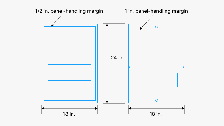
18 x 24 inches (457 x 610 mm): Very common in North America and Europe; this size provides a reasonable area with good handling, suitable for most fabrication and assembly equipment.
20 x 20 inches (508 x 508 mm): Now a common size for Europe, it gives a good square shape for some designs and layouts.
21 x 24 inches (533 x 610 mm): A bit more significant, it allows more boards on a panel to be run high-volume.
24 x 24 inches (610 x 610 mm): This measure is the largest of the standard sizes. The larger size has been popular all along but especially recently for very high-volume jobs because it reduces the number of times the manufacturing process has to be run and spreads the fixed costs of a run over more boards.
Actual figures may vary marginally depending on the capability of suppliers and specific manufacturing requirements.
Significance of PCB Panel Dimensions
Cost-Efficient: Optimal panelization ensures material use is minimized and the workspace used when processing a particular substrate utilization is maximized within any available manufacturing equipment. The common panel size lowers the cost associated with fitting the gadget well with the industry-standard equipment while minimizing the setup time and therefore upgrading the throughput time.
Ease of Manufacturing: Standard dimensions align with those supported by most PCB manufacturing factories, limiting incompatibilities to reduce production errors.
Control of Quality: Si principles of dimensioning benefit how manufacturers are able to handle dimensioned panels during the manufacturing process, which benefits the less likelihood of damage or introduction of defects to assure quality finished goods.
Optimal Layouts: Good use of panel space supports organizing many PCBs within a panel, which increases the yield and reduces scrap rates.
Factors influencing Selection of Panel Size
Although the standard dimensions make a very good starting point, the final decision in panel size could be influenced by several factors, among which are:
Board Size and Shape: The dimensions of the individual PCBs will naturally define the optimum size of the panel. Smaller boards can allow more flexible panelization than bigger or oddly shaped boards.
Volume Requirements: Increases in productivity realized by going with larger panels are due to high-volume runs and have proportionately less handling time per board, reducing the cost per board.
Equipment Capabilities : The available fabrication, assembly and testing machinery may have certain size limitations to be taken in to account.
V-Scoring and Routing Needs : The method used to separate boards from a panel can influence the layout. V-scoring permits greater cleanliness and less waste, routing might need more space between boards.
Edge Clearance and Tooling Holes: Edge clearance for handling and required tooling holes or fiducials may have an influence on the dimension of the total panels.
Assembly Constraints: Provision for the assembly process like pick-and-place machines and soldering needs to be present which ensures that there is enough space to get all the equipment properly in without a risk of damaging the boards.
Best Practice to Optimize a PCB Panel
Coordinate Early with the Manufacturer: Talk with the PCB manufacturer at the very early stage of designing to know what they are capable of doing and where their limitations are. This may help one minimize panel size and avoid potential problems.
Design Software Utilization: Specialized PCB design software can help efficiently lay multiple boards in a panel to optimize space and minimize any wastage.
Use Standard Board and Panel Sizes : Wherever possible, use common board and panel sizes to reduce costs and make the supply chain and production process easier.
Plan for Separation : Whether routing or V-scoring, spaces between boards should be considered so the boards can be separated cleanly without damage to the scored/cut PCBs.
Consider Handling and Transport: Ensure that the panel can be carried and transported by all operators and materials handling systems, from fabrication to assembly to final packing.
Test and Iterate: Have several different panel configurations prototyped to see which layout would work better based on your particular operation.
Tips for Getting the Most Efficiency
Select your most logical application methods to be assured that you will realize the highest value in terms of efficiency and cost savings:
Depaneling Router: Common but introduces dust and vibration, making this a selective tool for some.
Laser-Cutting Machines: With high precision and currently popular for smooth and clean cuts.
Hook-Shaped Blades: Cheap but not effective; however, still used when separating boards manually.
Combining Different Circuit Boards: To optimize on space and minimize the cost of a panel, you can combine different sizes and arrangements of the PCB.
Balancing PCB Panel Size and Board Thickness
The thickness and size of a PCB correlate with each other. Usage of the correct panel size with the thickness is very important in generating the perfect boarded product.
Standard Thickness: The industry-stand thickness is 0.063 inches, although 0.031 inches could be used for smaller applications and 0.093 inches for larger and more complex boards.
Dimensional Modifications: At times changing the board dimensions or their rotation also helps to accommodate more number of boards in order to realize effective material usage. It is highly applied in bringing more PCBs into a single panel either to minimize wastage of material or, in the end, to minimize costs.
Conclusion
The knowledge and effective use of standard PCB panel dimensions is very important for efficient, low-cost, and high-quality PCB manufacture. By careful considerations of what are all the parameters for panel size and close liaison with your manufacturer, your designs end up practical and for mass production. While standards for dimensions are lacking, they provide invaluable guidance to find the ultimate sweet spot that works best for your unique requirements by balancing performance, cost, and manufacturability. Whether it is simple single-layer boards you design or complex multi-layer circuits, careful planning and execution will let the finished product fully satisfy all necessary specifications and performance criteria.
Hot Tags:

Contact us

If you can't find what you're looking for, please contact us.
Article
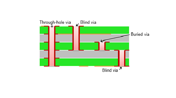
A printed circuit board includes a number of copper foil circuits, which are interlinked by vias. Via (through-hole, blind, buried, stacked, microvias) provides critical interlayer connections in high-density interconnection boards. Blind and buried vias increase the density of boards without adding size; hence, they are imperative for modern trends of miniaturization and high-speed signal transmission. These vias are plated with conductive materials, usually copper, so the electron flow can happen without much effort. Although advanced via types, like stacked vias, cost more, they save up much space and significantly improve routing capacity.
 2024/07/26
The article is developed concerning the breakthrough of integrated circuits and the need for custom PCBs in some electronic products. It enumerates ten golden rules in conducting PCB layout design and manufacturing: grid selection, routing, power layers, component placement, panel duplication, component value combination, frequent DRC, flexible silkscreen use, decoupling capacitors, and pre-production parameter checks. These rules provide for the optimum design and manufacturing of a PCB.
2024/07/25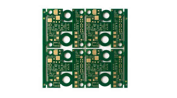
Most electronic circuits are mounted on PCBs, or Printed Circuit Boards, which provide mechanical support and electrical interconnection of electronic components. There are, however, special applications that involve the use of single and double-sided PCBs, multi-layer PCBs, or even rigid and flexible PCBs with aluminum backing, targeting medical, industrial, auto, and aerospace industries. They may use materials such as fiberglass, epoxy, aluminum, and others.
2024/07/25