- Products & Capabilities

- Simulation Design & EDA

- About
- Resources
Standard Size of PCB Vias


Vias in PCBs connect multiple layers and come in types like through-hole, microvias, blind, and buried. Proper sizing and design optimize PCB performance and reliability, aiding advanced device development.
Printed circuit boards are the backbone of modern electronic devices, integrating an enormous number of components into an effective, closely integrated system. Of all the most important aspects of PCB design, vias are small, conductive passages through which various layers of a PCB are interconnected. Knowledge of standard PCB via sizes and their applications aids in creating your electronic designs for optimal performance and reliability.
What are the Vias in a PCB?
Vias are small holes drilled into a Printed Circuit Board to provide electrical connections between layers. They become an essential factor in designs with multiple-layered PCBs, thus enabling complicated routing without increasing the actual size of the board while maintaining connectivity. Several types and sizes are available, each being designed for use in particular functions and design needs.
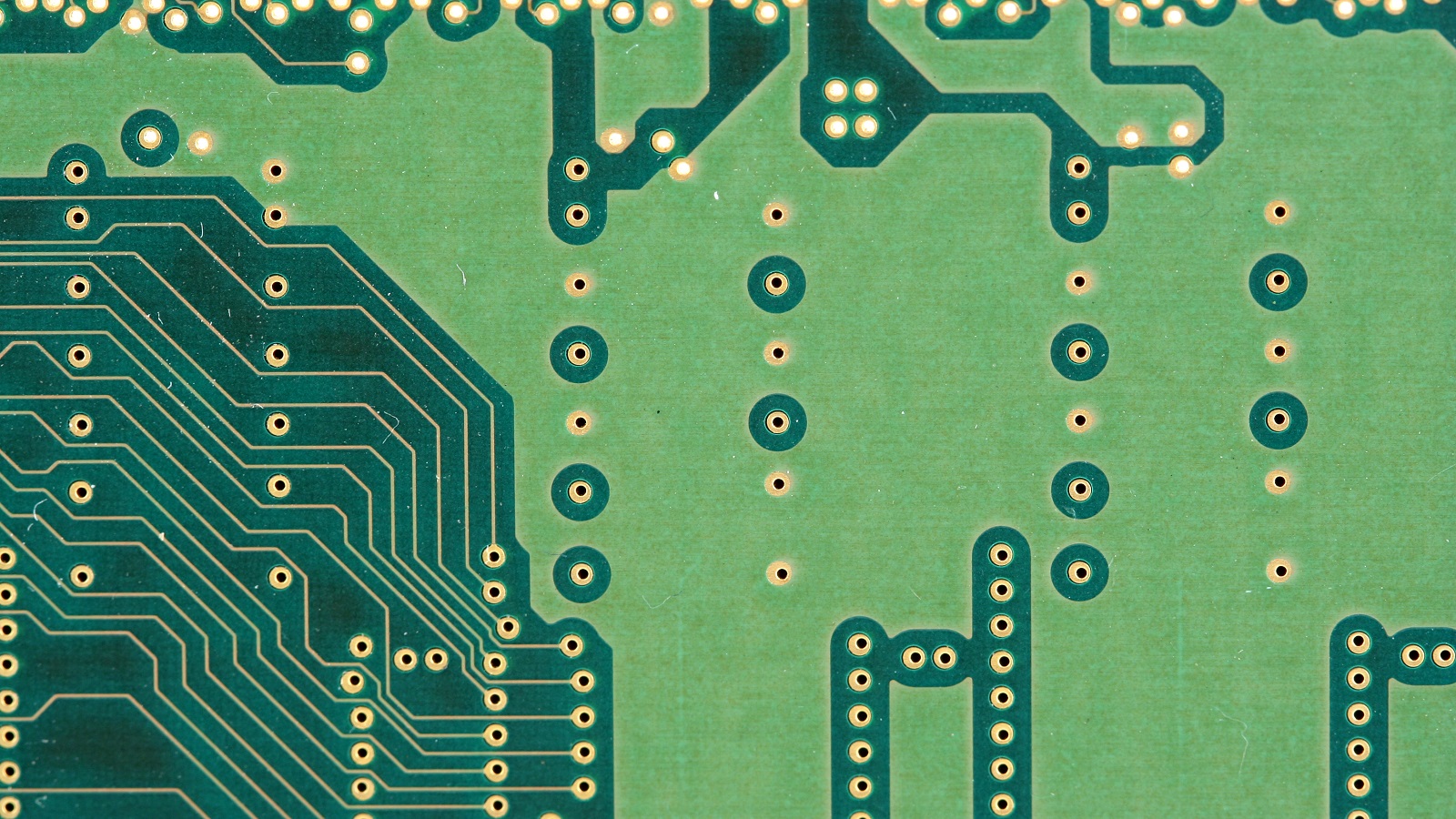
Standard Via Sizes
While most fabricators are slightly different, most PCB manufacturers offer standard via sizes. The following chart shows typical via sizes and hole dimensions by application:
Through-Hole Vias (PTH): These vias traverse the entire thickness of the PCB and connect the top and bottom layers, as well as internal layers.
Hole Diameter: 0.3 mm to 1.0 mm.
Pad Diameter: This is kept slightly larger than the diameter of the hole in order to make an effective annular ring.
Microvias: In HDI PCB, vias connect only two immediately adjacent layers.
Hole Diameter: Generally applied range is from 0.1 mm to 0.15 mm.
The Microvias thus offer tight spacing required for small-sized and high-speed designs.
Blind Vias: A blind via connects the outer layer to one or more inner layers without going through to the whole board. They call for precision drilling, thus increasing the complexity of fabrication.
Common sizes reflect those of through-hole vias but terminate within the board.
Buried Vias: Fully included within inner layers of the PCB, these vias do not reach any of the surfaces.
These can be comparable in size to microvias and help with layer stack refinement by keeping external space free of clutter.
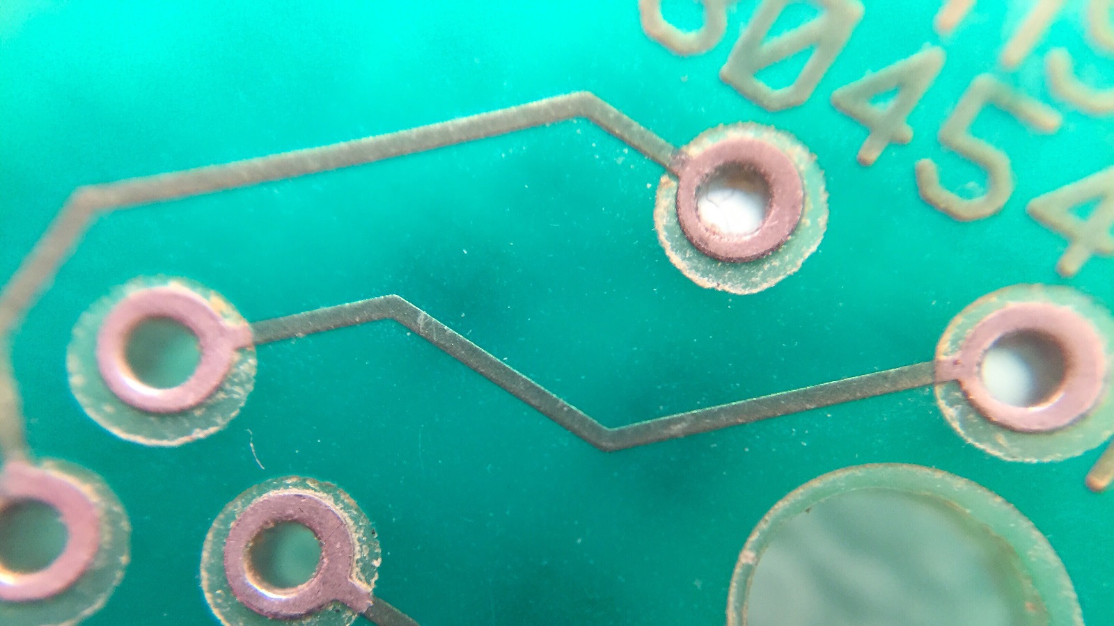
Via Size Calculation and Considerations
In calculating the via size for an application, it has to be considered based on a number of factors. These are application of the PCB, the layer configuration of the board, and electrical. The annular ring created by the copper pad surrounding it has to be taken into consideration. Normally, the optimal thickness of an annular ring is given by:
\[\text{Annular Ring} = \frac{\text{Pad Diameter} - \text{Hole Diameter}}{2 }
This will keep the drilled hole centered in the pad for maximum connectivity.
Factors Affecting Via Design
There are a number of prime variables, including but not limited to the following, that affect via design:
Aspect Ratio: this is the relationship between the PCB thickness and the via's drilled hole diameter. It defines plating reliability: the higher the aspect ratio, the more problematic the plating process.
Copper thickness: The usual practice is to have the via in the outer layer thicker, as it has to support higher value voltages. In the case of internal layers, thinner copper is possible since their particular electrical demands of the board should be very limited.
Manufacturing constraints: Each different PCB manufacturer has different fabrication capabilities and standards that affect availability via sizes and types. Designers should consult with fabricators early in the design phase so that they may align their specifications accordingly.
Via Filling and Plating Techniques
Various via filling and plating techniques are implemented in the design for different functionalities, which include:
Via Tenting: this technique is where the via is simply covered with a solder mask and not filled. Tenting via is fast, relatively inexpensive, but can reopen after some period, especially the tented vias.
Via Plugging: It means via plugging with a non-conductive material whose top is closed by a mask. It is used chiefly to avoid solder migration at the stage of assembly.
Via Filling (With Via-in-Pad): This is a process that concerns the complete filling of via with a conductive material, then copper-plating the surface and smoothening the resultant surface. Normally, this is done in high-density design where space is somewhat in shortage.
Electroplating: This is the well-controlled type of plating whereby via holes are internally coated with a conducting material, usually copper, by being subjected to an electrochemical bath. It ensures uniform distribution and is able to provide a good bond but may also be more expensive.
Advanced Via Design Considerations
Advanced via designs, such as sequentially drilled blind vias and depth drilling, play a role in advanced PCBs:
Sequenced Drilled Blind Vias: These vias are fabricated in a sequenced layer process, allowing for multilevel connections with more design freedom. Drilling and plating after layer bonding creates higher accuracy.
Depth Drilling: Refers to the process where un-used copper is removed from via stubs in order to minimize distortion of signals in high-speed applications, thereby enhancing signal integrity. Depth drilling has to be expertly planned by considering the depth against the usage of various different signal layers.
Conclusion
Understanding the normal size of PCB vias and their respective applications goes a long way in ensuring that PCBs are efficiently and reliably made. For example, such a balance of design requirements with fabrication capabilities means engineers can exploit vias to help achieve enhanced connectivity and board layout optimization in the interest of developing advanced electronic devices.
It is at this point, when structuring any new project with a PCB, that you make contact with established manufacturers to understand their specifications. Second, design your vias using current norms and technology in the industry. Advanced via strategies in design now give a good platform where innovation can occur concerning developments in this fast-evolving electronic field.
Hot Tags:

Contact us

If you can't find what you're looking for, please contact us.
Article

Annular rings are crucial for reliable PCB electrical connections. Proper sizing, understanding issues like tangency and breakout, and best practices ensure optimal performance and reliability in electronic circuits.
 2024/09/18
Pads and vias are crucial for PCB design: pads serve as soldering points for components, while vias connect different layers. Understanding and correctly implementing them ensures reliable, efficient, high-performance PCBs.
2024/09/16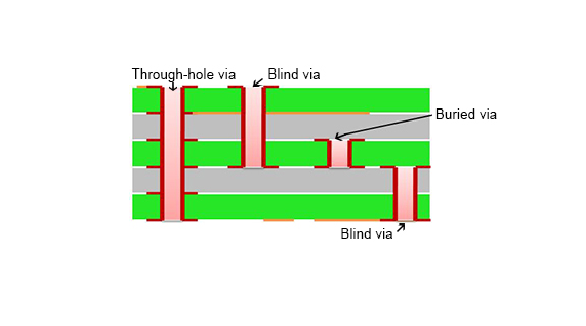
A printed circuit board includes a number of copper foil circuits, which are interlinked by vias. Via (through-hole, blind, buried, stacked, microvias) provides critical interlayer connections in high-density interconnection boards. Blind and buried vias increase the density of boards without adding size; hence, they are imperative for modern trends of miniaturization and high-speed signal transmission. These vias are plated with conductive materials, usually copper, so the electron flow can happen without much effort. Although advanced via types, like stacked vias, cost more, they save up much space and significantly improve routing capacity.
2024/07/26