Standard Thickness of PCB
PCB thickness is crucial in electronics, influencing performance, durability, and cost. The standard thickness is 1.57mm, but other sizes exist for specific needs. Factors like copper thickness, material choice, layers, and environmental conditions determine suitability. Custom thicknesses cater to high-power, space-limited, and high-frequency applications but may increase cost and production time. PCBX offers various thickness options, emphasizing quality and customer service in PCB manufacturing.
Printed circuit boards are the unsung heroes of modern electronics, hidden under the hood of every gadget, from a smartphone to a satellite. At the heart of designing and fabricating a printed circuit board is the choice of its thickness, which affects the performance, durability, and cost of the board. While there isn't an absolute industry standard for the thickness of a PCB, there are some baseline measurements preferred and in use today due to historical and functional advantages associated with their application. This article explores what determines the thickness of a PCB, how the thickness affects both performance and manufacturing, and what considerations go into deciding whether to use a non-standard custom thickness.
Common PCB Thicknesses
The most widely accepted standard of PCB thickness is 1.57 mm (0.062 inches). This size dates back to the early days of PCB fabrication where Bakelite sheets were made at this thickness. Over the years, this dimension has remained predominant due to the evolution of manufacturing processes and equipment calibrated to this size.
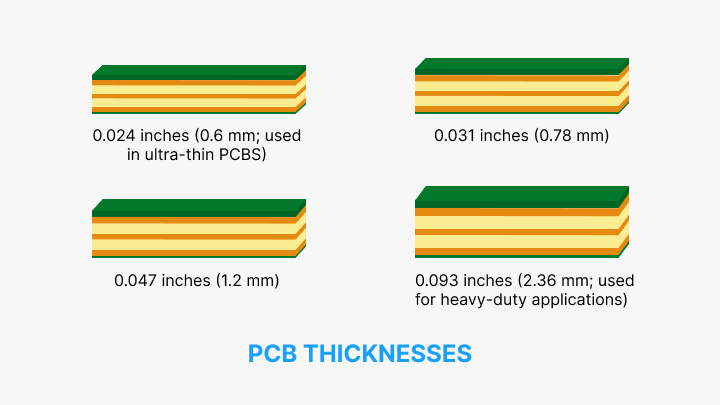
Other common thicknesses apart from the standard 1.57 mm have only recently gained popularity in order to accommodate specific applications:
0.024 inches (0.6 mm; used in ultra-thin PCBs)
0.031 inches (0.78 mm)
0.047 inches (1.2 mm)
0.093 inches (2.36 mm; used for heavy-duty applications)
Measuring the Thickness of a PCB
There is quite some precision required in measuring the thickness of a PCB, employing various tools like a micrometer, calipers, and, for higher accuracy, non-contact methods that include laser micrometers and optical profilers. All these tools are essential in verifying whether the manufactured PCBs meet the specifications in the design.
Factors That Affect the Thickness of a Printed Circuit Board
There are various design and manufacturing factors that determine a suitable thickness for a PCB.
Copper Thickness
Copper thickness is always expressed in ounces per square foot and plays a very important role in the current-carrying capacity and thermal performance of the board. The common ranges of copper thickness vary from 1 to 2 oz, which in turn affects the overall thickness of the PCB and also the complexity in manufacturing. Higher copper content requires thicker boards capable of handling increased thermal dissipation and current loads.
Material Choice
The substrate and laminate materials also drive PCB thickness. Typical substrates include epoxy resin, glass weave, or ceramic, while laminates consist of thermoset resin. With distinct thermal, mechanical, and electrical properties, each material impacts the overall integrity and functionality of the board.
Number of Layers
The more the number of layers on a PCB, the thicker it is. A standard 1.57 mm thick PCB can have 2 to 6 layers easily. However, in multi-layer boards, sometimes the number of layers goes beyond 60, and each extra layer adds to the thickness considerably. Decreasing the number of layers is sometimes not a feasible option, especially in complicated designs, and this brings extra thickness.
Size, Weight, and Flexibility
The eventual application of the PCB greatly impacts the thickness requirements. The rigid ones require larger profiles to enhance durability, and the flexible ones should be thin enough to ensure they retain their flexibility, which is a crucial factor in their existence. The right balance between rigidity and flexibility is of essence in the decision on either one. It is based on the environmental working condition the board is exposed to.
Environmental Conditions
Under harsh environmental conditions, like high temperatures or mechanical stress, the thicker PCBs are more resistant. However, thinner PCBs are used for reducing weight in compact or portable devices.
Impact on Manufacturing
The choice of the PCB thickness does not only influence the electrical and mechanical features of the board, but it also impacts several aspects of manufacturing:
Drill Hole Equipment
Thicker PCBs need more advanced drilling equipment since it can sustain precision, and the hole diameters below become difficult with increasing thickness.
Copper Etching
A thicker copper layer complicates the manufacturing processes like etching, thus making the manufacture costlier and the production more challenging.
Depanelization Method
The method of depanelizing individual PCBs from the panel depends on the thickness. Thick boards are usually V-scored because they are rigid, but thinner boards may use breakaway tabs.
Custom PCB Thickness
While a standard thickness works most of the time with almost all modern manufacturing processes, certain applications mandate the use of custom thicknesses like:
High-Power Applications: These use thicker boards that can handle current and deal with heat generation.
Space-Constrained Devices: This would be the case with smartphones, where a thinner PCB might realize a notable design advantage.
High-Frequency Applications: In such applications, thinner boards lower signal loss, improving performance.
Rugged Environments: In such applications, extra mechanical ruggedness and durability are needed.
There are various factors that must be considered in choosing custom thickness:
Manufacturing Capabilities: This is to establish the limitations of available equipment at the manufacturer and their process capability.
Turnaround Time: Custom thicknesses may prolong production time while the manufacturing processes get adjusted.
Added Expenses: Special thicknesses normally cost more because of specially required materials and longer production time.
PCBX: Your Best Partner in Diverse PCB
PCB Thickness: PCBX offers a variety of PCB thickness options well beyond standard options, so you get all the functionality you may need in one for your unique application. Standard choices, while faster and more cost-effective to manufacture, can turn into custom thicknesses to make sure it fits your application to a T.
At PCBX, we strive to give our customers the best PCBs every time. Whether it is the type or volume of printed circuit boards you wish to order, customer service and expert engineering are the cornerstones of our business that ensure our products are well-made and competitively priced.
With PCB manufacturing facilities in both the domestic and international markets, PCBX has served customers worldwide. Feel free to contact us if you are interested in tapping into what we can do, or have questions about discussing various PCB thickness options.
Hot Tags:
Contact us

If you can't find what you're looking for, please contact us.
Article
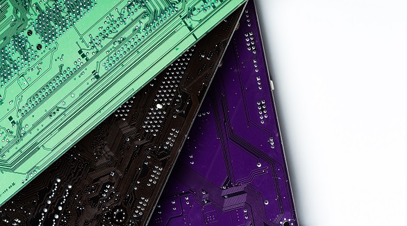
Solder masks protect PCBs from environmental damage and electrical shorts, enhancing reliability and aesthetics. The application is complex, requiring professional fabrication to ensure quality and compliance with regulations.
PCBs (Printed Circuit Boards) are fundamental in electronics, composed of multiple layers like silkscreen, soldermask, copper, and substrate, chosen for specific electrical functions.
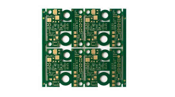
Most electronic circuits are mounted on PCBs, or Printed Circuit Boards, which provide mechanical support and electrical interconnection of electronic components. There are, however, special applications that involve the use of single and double-sided PCBs, multi-layer PCBs, or even rigid and flexible PCBs with aluminum backing, targeting medical, industrial, auto, and aerospace industries. They may use materials such as fiberglass, epoxy, aluminum, and others.