- Products & Capabilities

- Simulation Design & EDA

- About
- Resources
Through-Hole (THT) Assembly PCB Design Rules


Through-hole assembly is a key PCB manufacturing technique offering reliability and mechanical strength. This article details design elements, requirements, and standards, including thermal pads, IPC performance levels, component types, solder joint quality, hole sizes, and annular ring dimensions, ensuring robust and manufacturable PCBs for various applications.
Through-hole assembly is still one of the predominant techniques in the manufacturing of PCBs, and the reason is that it offers high reliability and mechanical strength. Thus, whether one designs for consumer electronics or the high-reliability system domain, through-hole assembly design rules ensure performance and manufacturability. This article is all about design elements, requirements, and standards for through-hole assembly.
Thermal Pads
Thermal connections are the most significant part in determining a good soldering and thermal management. These connections follow a spoke-like pattern, like spokes on a bicycle wheel, from the leadless pad to the copper plane or foil. The main purpose for such spokes is to balance the thermal dissipation of the copper area, such that when properly soldered, the copper does not draw away too much heat, but the thermal pad has not been squashed at the expense of current-carrying capacity. The diameters of such thermal pads are to be in keeping with internal pad diameters: the sum total of all the spokes' widths is the diameter of the pad. It is the total area that covers the pad and its spokes, and the value is 1.5 times the pad's inner diameter.
Performance Levels
IPC standards classify PCBs into three classes based on various levels of complexity, functionality, and reliability requirements:
- Class 1: This class covers all products coming under general consumer electronics and a few low-reliability items. A lot of product categories that fall under this class are general types of consumer products and other types of computer peripherals.
- Class 2: Better performance and more reliable nature electronics, for example – communication equipment, business machines, and military instruments. Independent occasional failure rates are okay to have in these applications.
- Class 3: High-reliability electronics. Critical commercial and military systems fall into this class. System failures are unacceptable in this class of, and availability is of utmost importance.
Through-Hole Assembly
Component Types
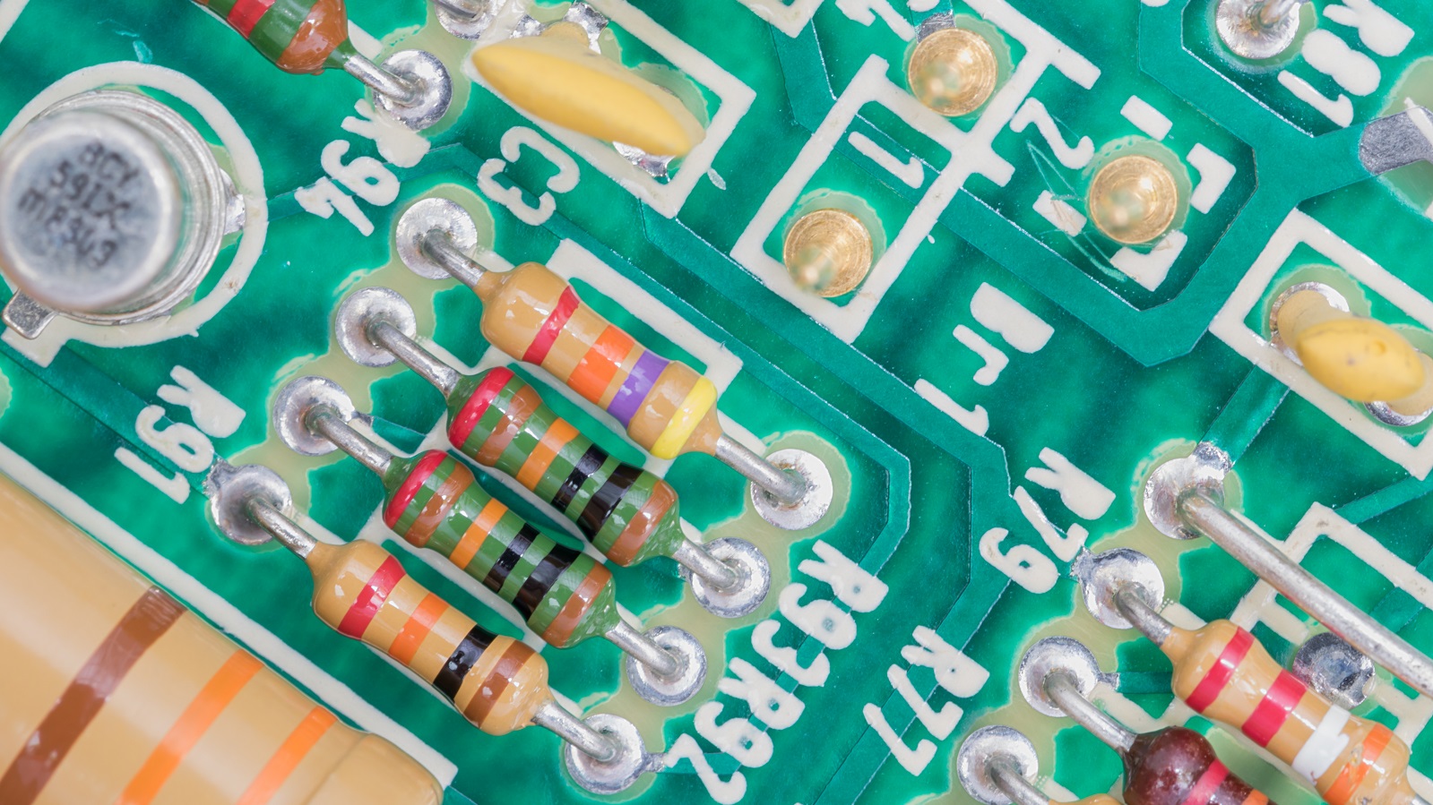
Axial Leads: This implies that components have leads entering and exiting on the opposite sides. They allow lead spacing, which is variable.
Radial Leads: These have leads that go in and come out from the same direction. They usually consume less board size while at the same time not providing adjustability for the lead-to-lead pitch.
Solder Joint Quality
Strong good solder joints are the key elements in the reliable electrical interconnection between the leads and the PCB. All solder joints should be verified for proper joint strength and the absence of defects.
Drill Hole Size
Hole and pad sizing are important to maintain strength and the ability to form a solder joint. The target drill hole sizes are:
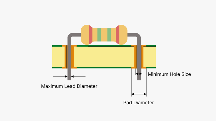
- Density Level A: Min hole size = Max lead diameter + 0.25 mm
- Density Level B: Min hole size = Max lead diameter + 0.20 mm
- Density Level C: Min hole size = Max lead diameter + 0.15 mm
Annular Ring Size
The annular ring should have a fair width for a sound solder joint. For through-hole components, the pad diameter shall be made as follows according to IPC-2221:
Density Level A: Pad Diameter = Minimum Hole Size + 0.1 mm + 0.6 mm
Density Level B: Pad Diameter = Minimum Hole Size + 0.1 mm + 0.5 mm
Density Level C: Pad diameter = Minimum hole size + 0.1mm + 0.4mm
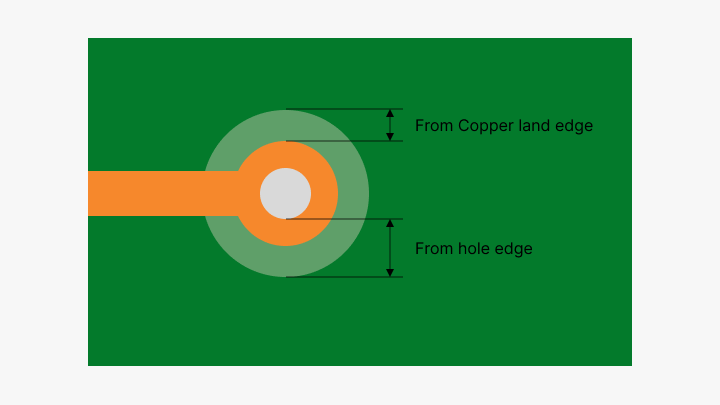
Solder Mask Relief
Solder mask relief usually conforms to a general tolerance of 4 mils (0.1 mm) around the pads or annular rings. This rather liberal space gives room for appropriate soldering without bridging.
Solder Fill
Though 100% fill of the solder is the preferred option, often a rate of fill of 75% is acceptable for both Class 2 and Class 3 boards. In this way, mechanical strength and thermal conduction is gained by reducing surplus solder.
Clearance and Separate Drill Files
Sufficient clearance in the holes ensures a good flow of solder and rules out dual-side soldering, which is time-consuming. Always provide a separate drill file for plated-through holes (PTH) and non-plated-through holes (NPTH) to avoid conflict during manufacturing.
Component Mounting Order
Mount the flatter and smaller components first, then as you go along, increase to the larger and taller components. This kind of ordering will help to sustain efficiency and can rule out obstacles in the mounting process.
Other Design Considerations
- Masking Tapes: Masking tapes can be applied on the short component leads to allow for easy bending.
- Conformal Coating: Apply conformal coatings to prevent corrosion.
- Potting: Utilize potting methods to provide mechanical and electrical stability.
- RoHS Compliance: The manufacturer shall support Restriction of Hazardous Substances with regard to environmental protection.
Thermal Considerations
- Even heat distribution is important during proper soldering. The leads and pads should have even heating so that the solder sticks to them. Take notice of the parasitic capacitance and inductance involved in conventional designs on PCB, of which high-density board design is imperative.
Specifics for High-Density Designs
- For high-density requirement boards, choose through-hole diameters as follows: Via: 0.20 mm, pad: 0.46 mm, isolation area: 0.86 mm.
- Indeed, inductance can be improved by placing through-holes close to power and ground pins, which helps in overall performance and reliability.
- By adhering to these guidelines on through-hole assembly design, a PCB designer can have robust, reliable, and manufacturable PCBs that comply with the performance criteria their application requires. All of these best practices are at the heart of effective and efficient through-hole PCB design and assembly, ensuring in-production and in-field success.
Hot Tags:

Contact us

If you can't find what you're looking for, please contact us.
Article
Printed Circuit Board Assembly (PCBA) employs Through-Hole Technology (THT) and Surface Mount Technology (SMT). THT offers robust mechanical bonds, ideal for high-stress applications, whereas SMT supports efficient, high-density assemblies. Each method has unique advantages and limitations, impacting cost, manufacturing efficiency, and component compatibility. Understanding these differences is key for optimal PCB design.
 2024/09/11
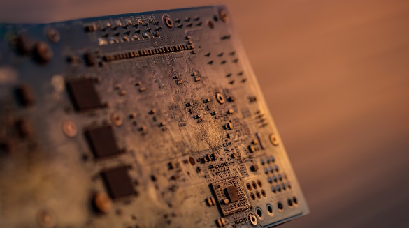
PCBs are central to electronic devices, featuring holes and vias critical for functionality. Holes, like through-holes and mounting holes, serve electrical or mechanical purposes, while vias ensure electrical connections across PCB layers. Understanding their differences is key for optimal performance, reliability, and manufacturability in PCB design.
2024/09/11
PCBs are essential for electronic devices, providing mechanical support and electrical connections. This article explores the importance of PCB panel dimensions, standard sizes, and optimization techniques. Key points include cost-efficiency, ease of manufacturing, quality control, and optimal layouts. Factors like board size, volume needs, and equipment capabilities influence panel size. Coordination with manufacturers, using design software, and employing standard sizes can enhance production efficiency and quality.
2024/09/11