Transparent PCB
Transparent PCBs combine aesthetics and functionality using advanced materials, enhancing electronics and offering diverse applications despite high costs and complexity.
The electronics industry is one that works on innovation and betterment in performance and aesthetics of gadgets. In addition, the development of Transparent Printed Circuit Boards has placed them at the edge of this change, merging visibility with performance. Such see-through PCBs will be made using advanced materials and techniques that are opening up new frontiers for applications across different sectors. This article serves as an overview of transparent PCBs in terms of their materials, advantages, challenges, and uses to show how they're beginning to revolutionize electronic design.
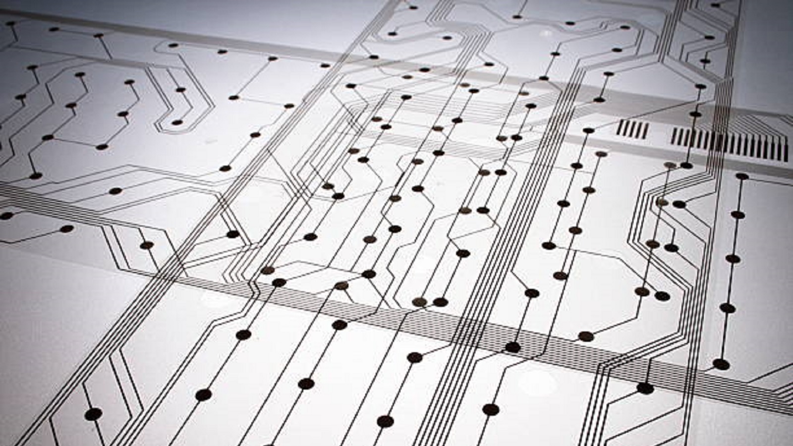
A transparent PCB is a circuit board that allows light to pass through, showing its internal components while still being functional. These boards use materials such as glass, ceramic, polyimide, and polyester to achieve transparency. The pathways and components can be fully or semi-transparent, offering a set of unique advantages and aesthetic appeal. Transparent PCBs are especially relevant in the context of 5G networks, where they might change the face of digital communication.
Materials Used
Glass: Glass transparent PCBs use tempered or sapphire glass due to the excellent transparency of glass. These materials make them very durable and highly thermal-resistant. These are very suitable for LED displays and optical devices, offering environmental friendliness due to their recyclable properties.
Ceramic: Made up of aluminum oxide and magnesium oxide, ceramic transparent PCBs boast better thermal conductivity and resistance. Hence, they are quite handy for high-power applications. Though providing only slightly less transparency compared to glass, its robustness can support such demanding applications as high-power LEDs or infrared windows.
Flexible Materials: Polyimide and polyester make up flexible transparent PCBs. Offering around 95% transparency, these materials are perfect for flexible, bendable, and three-dimensionally shapable applications, such as wearable electronics and smart textiles.
Manufacturing Process
The steps of transparent PCB manufacturing are done in detail:
Materials Selection: Select appropriate material based on desired properties and applications,
Design Layout: Prepare, and print the circuit design layout
Substrate Fabrication: Fabricate substrate by using transparent materials,
Copper Application: Apply Copper foil and photoresist,
Expose to Light Sources: Provide boards to light sources that will develop photoresists,
Etching Process: Unwanted copper will be removed by Ferric Chloride.
Final Cleaning: After processing is complete, the PCB will need to be washed and then dried.
Following all design guidelines-like trace length and noise filtering components-is crucial for better performance.
Advantages and Disadvantages
Advantages
Attractiveness: With transparent PCBs, innovative designs can be visualized that offer an exquisite see-through look.
Diverse Usage: They can be fit into smaller spaces, therefore increasing device functionality without affecting the fashionable aspect.
Material Usages: Provide excellent heat resistance, durability, and recyclability essential for ecological concerns.
Disadvantages
Higher Cost: The manufacturing of transparent PCBs is more expensive than for traditional PCBs, since the materials and processes used are more advanced.
Thermal Limitations: Some of the available materials for transparency cannot resist higher temperatures as their conventional alternatives do.
Manufacturing Complexity: Such PCBs need very specific production expertise, and scaling operations might be problematic.
Applications
Transparent PCBs can be found in the following areas of application:
Consumer Electronics: Aesthetically appeals and offers more value in smartphones, tablets, smartwatches, and other wearable electronics.
Automotive Industry: Applied in complicated dashboard interfaces and ambient lighting systems for aesthetic advantages.
Medical Devices: Allow for inconspicuous and smooth integration into wearable health monitors and diagnostic devices.
Fashion and Textiles: Driving the use of electronic fabrics, embedding technology without sacrificing fashion.
Challenges in Transparent PCB
Despite the promising advantages of transparent PCBs, they do have a number of challenges:
Cost and Production: Higher manufacturing costs and complicated fabrication methods remove their widespread use in budget or low-end products.
Durability Concernations: Transparency in material has to be taken cautiously for durability with high-stress conditions.
Limited Availability: Since it is a niche technology, skilled manufacturers or suppliers are hardly available.
The future is bright for transparent PCBs, considering the present challenges. Material science and manufacturing processes are very likely to reduce costs over time and make transparent PCBs more available, hence spread wider.The integration of these technologies into a wide range of sectors will accelerate as they continue to develop, bringing appeal and new functions.
Transparent PCBs are redefining electrical design by combining the most cutting-edge technology with a visible element. It may have a significant impact on anything from consumer electronics to automobile innovation. Transparent PCBs are now in a position to drive future developments and keep transforming electronics thanks to further advancements.
Hot Tags:
Contact us

If you can't find what you're looking for, please contact us.
Article
LED PCBs power modern lighting with efficiency and adaptability, ideal for diverse applications. Their design emphasizes thermal management, cost-effectiveness, and versatility, driving sustainable illumination solutions.
Gold recovery from circuit boards needs safety gear, precise dismantling, cleaning, etching, and filtering, crucial for safe e-waste recycling.
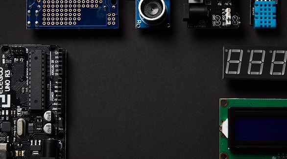
Breadboards and protoboards are key prototyping tools in electronics. Breadboards allow for flexible, solderless circuit design, while protoboards provide durable, soldered connections for finalized designs.
