Types of Fuses
Fuses protect electrical systems from overcurrent, preventing damage and fires. Various types suit different applications, requiring careful selection for safety.
In modern electronics, compact and efficient component needs continue to increase, thus yielding innovative solutions like Mini-MELF diode boards. These boards integrate the miniature version of Metal Electrode Leadless Face, commonly known as MELF diodes, which are robust and reliable. For high-density applications, Mini-MELF diode boards are designed to avail a bundle of advantages to space-constrained and high-performance environments. This article throws light on the characteristics, applications, and emerging trends related to Mini-MELF diode boards.
Mini-MELF diodes, also known as SOD-80 diodes, come in a cylindrical form factor and compactness of size. The peculiar packaging does without the leads on the outside, making it surface-mount. In application on PCBs, the Mini-MELF diodes are leadless and keep all electrical features as their conventional through-hole counterparts but with much-reduced size.
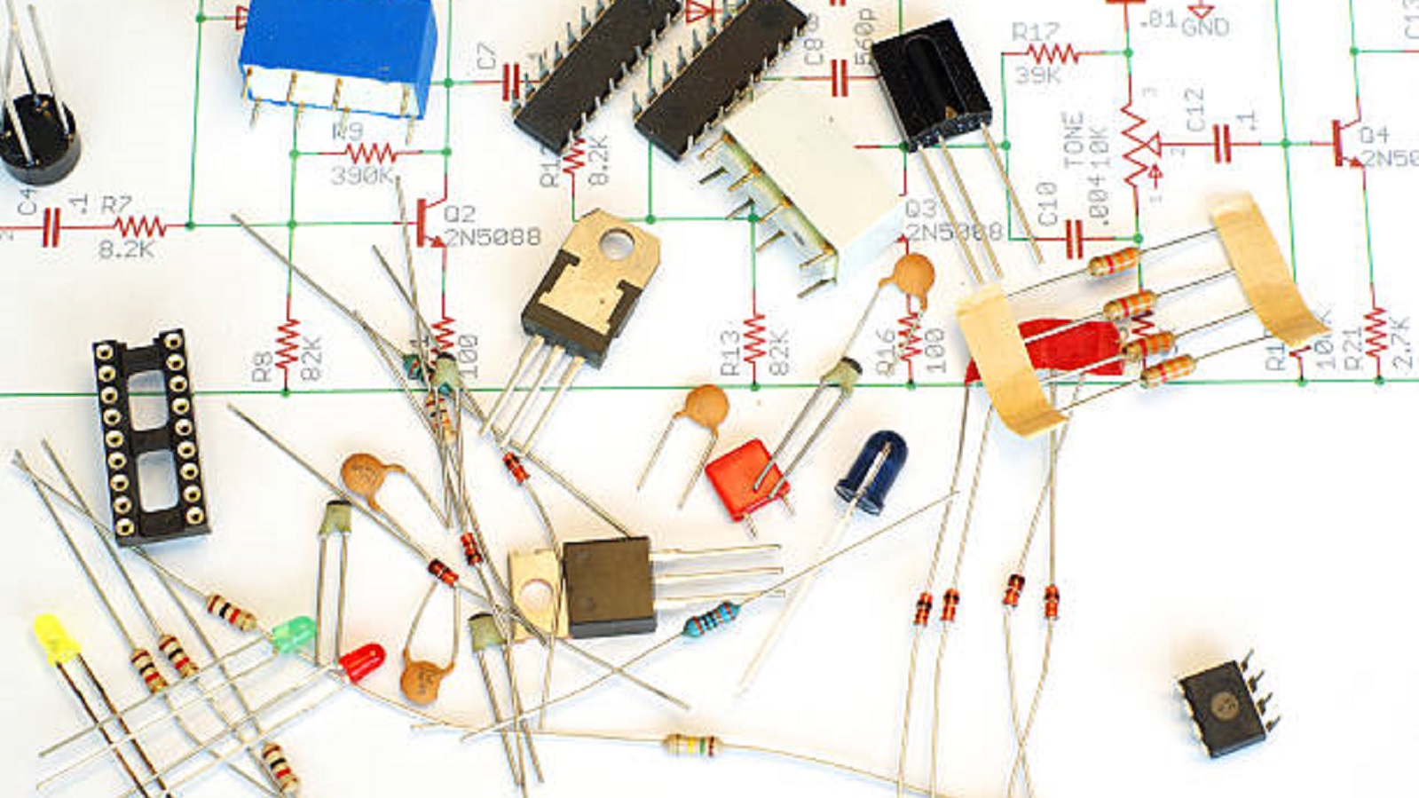
Key Benefits of Mini-MELF Diode Boards
Space Efficiency: Mini-MELF diodes are 90% smaller than standard through-hole diodes, thus providing the possibility of placing more components on a given area of PCB. The compact size is excellent for modern, tightly filled circuit boards where space-savings are essential.
Low Profile: With heights often under 1 mm, Mini-MELF boards enable ultra-slim electronic devices and modules in design, along with innovative form factors.
Improved Reliability: The strong structure of Mini-MELF diodes, especially solid construction with finished solder joints, leads to better mechanical stability and reliability. This construction provides safety to the diode chip from physical and environmental damage for a long time.
Higher Efficiency: The smaller internal lead lengths in Mini-MELF diodes reduce parasitic impedances, allowing higher operating frequencies and faster switching speeds.
Simplified Assembly: This surface-mount design is compatible with automated pick-and-place systems for increased manufacturing speed while decreasing the possibility of human assembly errors.
Types of Mini-MELF Diode Boards
Mini-MELF diode boards can be fabricated to suit different applications and use various characteristics of the diodes:
Rectifier Boards: These contain diodes arranged in configurations like single diode, bridge, or center tap to convert AC to DC, common in power supply units.
Voltage Regulator Boards: These use Zener diodes for voltage stabilization to protect electronic circuits against fluctuation.
Protection Boards: These are designed to save the circuits from adverse conditions such as reverse voltage, overcurrent, and electrostatic discharges.
Logic Gate Boards: These incorporate diodes into simple digital logic circuits to perform basic operations such as AND, OR, and NOR gates.
Mixer/Multiplier Boards: These use diodes combined with op-amps in order to process and combine analog signals; common in RF and communication systems.
Composition of a Mini-MELF Diode Board
Each Mini-MELF diode board, despite its application-specific variations, includes several core elements:
PCB Substrate: The base layer providing structural support and electrical pathways, usually made from FR-4 epoxy for rigid boards or flexible materials for adaptable designs.
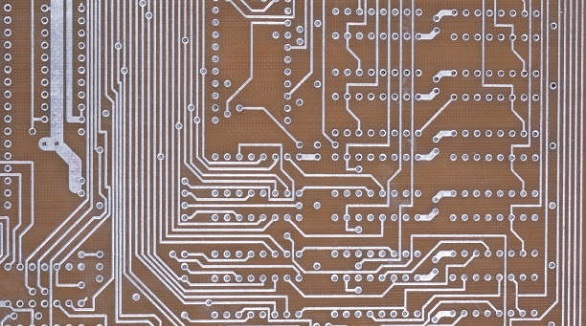
Copper Traces: These are etched pathways that connect components, thus enabling signal routing across the board.
Solder Mask: This is a protective layer that prevents accidental solder bridges and oxidation, hence preserving the perfection of solder joints.
Silkscreen: This overlay is used for labeling components and indicating polarity, among others, for easy visual guidance on the board during assembly.
Diodes: These are the main active components, whose functions range from signal rectification to voltage regulation; they may be Schottky or Zener types.
Supporting Components: These may include resistors, capacitors, or transformers, depending on the intended use of the board.
Manufacturing Process of Mini-MELF Diode Boards
Manufacturing a Mini-MELF diode board requires up-to-the-minute detail in various touches, amalgamating art in design with technology at its best in production:
Design: Engineers use CAD software to create schematic layouts and simulate electronic performance in pursuit of functionality.
Material Procurement: High-quality substrates, copper foils, and component reels are procured to meet stringent specifications.
Photolithography: Done with a photosensitive film where the unexposed areas, after development, are etched away to create the copper trace pattern. The film protecting the traces is stripped off and the copper traces are etched and finalized to show the way.
Solder Mask and Silkscreen: Additional protective and informational layers are applied to assist in the assembly and to make sure the board endures.
Component Placement and Soldering: Automated machines place components onto the board, followed by reflow soldering to secure parts through precise heating. Testing and Inspection: Rigorous quality checks confirm that boards meet electrical and mechanical specifications before distribution.
Applications of Mini-MELF Diode Boards
Mini-MELF diode boards find utility across diverse applications, offering tailored solutions in various sectors:
Consumer Electronics: Smaller size is decisive for smartphones and tablets; voltage regulation, power rectification are functions provided.
Automotive Electronics: They find applications in systems where performance needs to be strong under variable temperatures and vibrations, like control modules and sensor networks.
Telecommunications: These are used in high-frequency circuits where low parasitic impedances and high switching speeds are extremely important for signal integrity.
Industrial Equipment: Operating in very demanding environments, these devices ensure reliability in power management and safety systems.
Future Trends for Mini-MELF Boards
With the rapid advancement of technology, Mini-MELF boards are bound to meet the demands that are emerging due to the following trends:
Higher Current and Temperature Ratings: Developments are foreseen to increase the current-handling capability and thermal resilience of Mini-MELF diodes.
Semi-Additive Processes for Increased Density: The innovative processes in the manufacturing of PCBs will enable more intricate designs and denser circuit pathways.
Integration of Embedded Magnetics: Studies regarding inductors and transformers inside PCB layers will revolutionize board functionality and space efficiency.
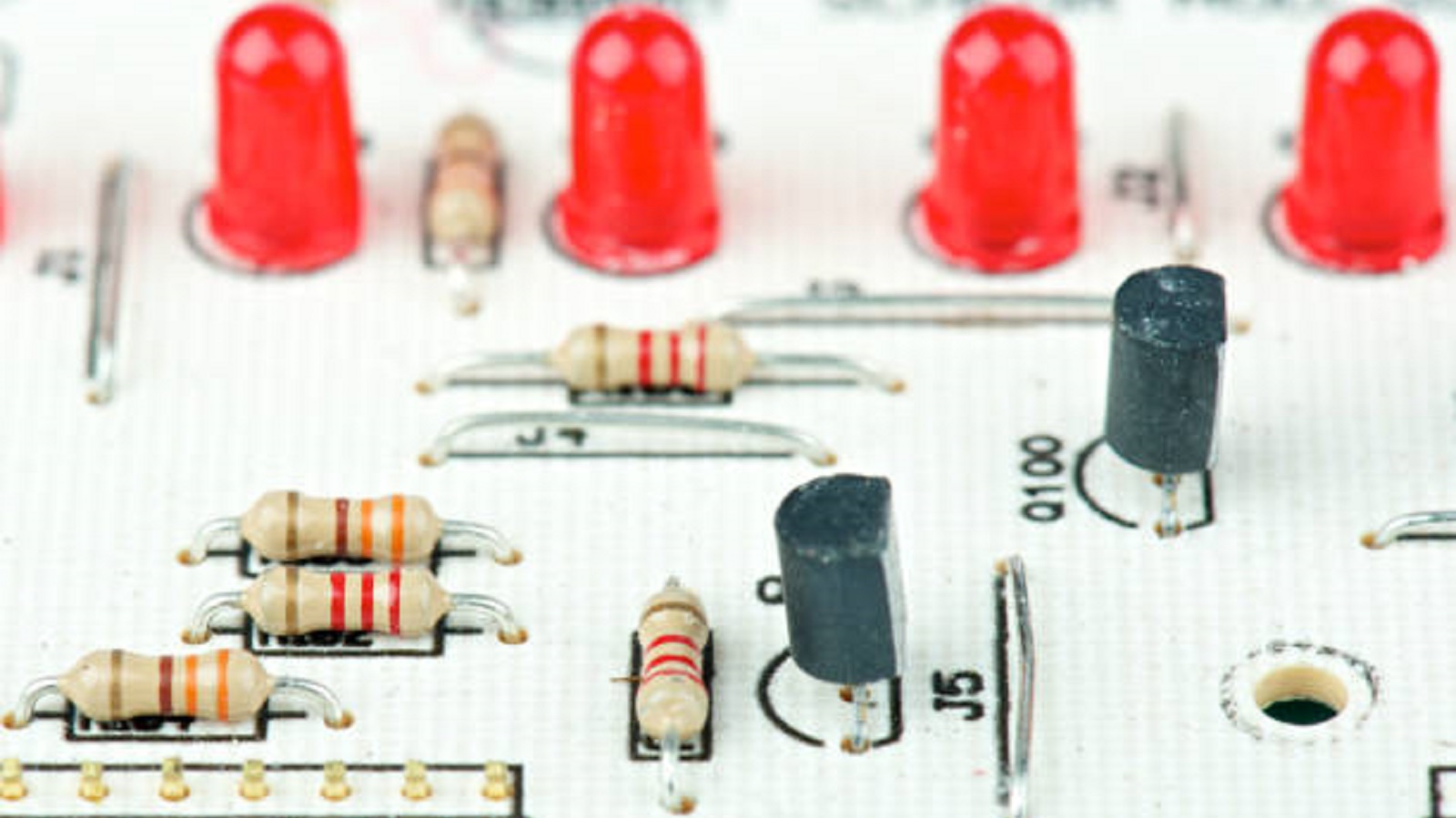
Mini-MELF diode boards speak of the evolution in design for compactness, high efficiency, and reliability. Low-profile, durable, easy-to-assemble, Mini-MELF diodes mean that engineers are now in a position to really develop a printed circuit board with state-of-the-art needs. Moving into the future, further developments will certainly extend the scope of using Mini-MELF boards to solidify their position in the future of electronic design and manufacturing.
Hot Tags:
Contact us

If you can't find what you're looking for, please contact us.
Article
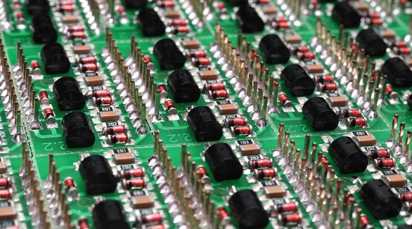
Burn-in boards are vital for testing semiconductor reliability, simulating stress to reveal defects, ensuring high-quality devices before mass production.
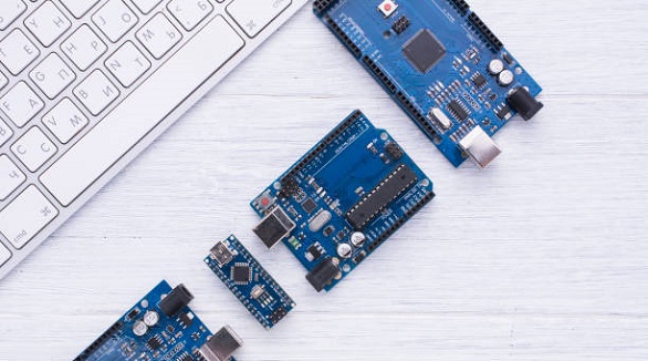
Arduino Nano and Micro differ mainly in USB capability and I/O options, with Nano suited for simple projects and Micro for USB-intensive, compact applications.
Select aluminum PCBs for excellent heat management or FR4 PCBs for cost-effective versatility in diverse electronic applications.
