Types of PCB Pad
PCB pads connect components on circuit boards. Understanding through-hole, surface-mount, and BGA pads is key for effective PCB design and manufacturing.
The pads are considered the critical components of the circuit because, through the assistance of bonding sites, they offer the essential connection between the component leads on the printed circuit board. Comprehending types and applications of different varieties of pads is crucial for professionals involved in the process of PCB design and manufacturing. This article will help one understand the world of PCB pads specifically solder pads, smd pcb boards, and other key elements pertaining to pad types.
What is a PCB Pad?
A PCB pad can be described as a certain revealed area of copper on the printed circuit board, at which the lead of the component is soldered. A pad is the fundamental allowing electrical interconnectivity between components that influence solderability, stability, and heat management. Generally speaking, the classification of pads can be made in two forms: through-hole pads and surface-mount pads, each with different components and packaging ways.
Through-Hole Pads
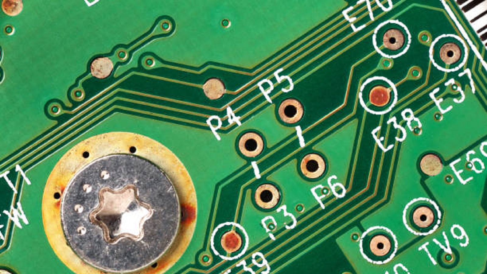
Through-hole pads are intended for mounting of components with leads, which go through the board. These pads require that the lead is inserted through plated via holes. The connection through through-hole solder pads is mechanically robust; therefore, suitable for application where there is a higher possibility of stress.However, on multilayer PCBs, the extensive usage of through-hole pads might limit the available routing space due to the component leads and vias required for them.
Surface Mount Pads

Surface mount pads are particularly intended for components that should be mounted directly to the board's surface. In this respect, they are part and parcel of such smd pcb board design since the latter provides for high-density layouts with increased functionality without having to turn to larger boards. On the other hand, however, surface mount solder pads can hardly accommodate those components which generate a lot of heat, besides perhaps calling for more precision in soldering.
Ball Grid Array (BGA) Pads
BGA pads require superior design considerations since they connect BGA-style components. Two of the major types of BGA pads include solder mask-defined pads or simply SMD and nonsolder mask-defined pad, shortened as NSMD.
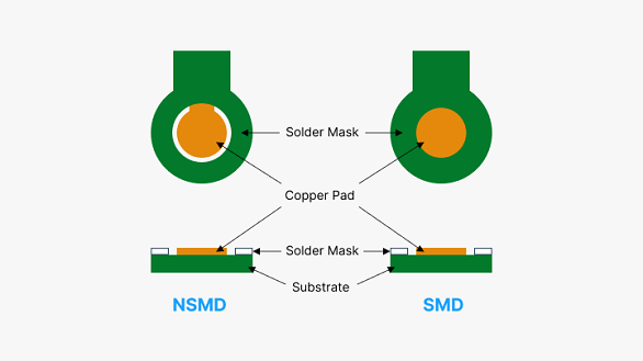
Solder Mask Defined Pads: These are of the type where the solder mask overlaps the copper pad slightly. These pads provide stability to the pad in terms of movement and offer accurate positioning for BGA components. On the other hand, the configuration of SMD pads is somewhat predisposed to limiting the space available for routing tracks and through-holes.
Non-Solder Mask Defined Pads: These are pad sizes defined by the copper diameter, allowing for a small clearance between the pad and the solder mask. It follows that NSMD increases the available surface area for solder joints; therefore, they have become a standard for high-density fine-pitch applications. Inasmuch as NSMD pad technology has many advantages, its applications can be prone to problems in delamination under both thermal and mechanical stress.
Other Pad Types
Lead Pads: Lead pads are applied to components with leads protruding for consistent solder connection.
Aperture Pads: The aperture pad can be defined as that particular opening in the solder mask, showing the underlying copper pad, which aids in determining how effectively the solder material attaches itself to the pad during the board assembling process.
Thermal Pads: Functional elements with high heat output require thermal pads in order to provide a channel whereby the heat may be distributed across to broader copper areas or connecting layers.
Selection and design of PCB pads are crucial in terms of the functional integrity and manufacturability of printed circuit boards, whether it involves solder pads for through-hole components or surface mount design on smd pcb for optimal results. Several types of pads serve different electronic and mechanical purposes. By offering options such as different aperture pad configurations for BGA pads, the designer is best able to design with options that best suit the specific operational needs at hand while considering nuances of size, heat, and stress.
Hot Tags:
Contact us

If you can't find what you're looking for, please contact us.
Article

Solder masks protect PCBs from damage and solder bridging. Available in various types and colors, they ensure reliability. Eco-friendly options and precise thickness measurements are crucial for quality.

Pads and vias are crucial for PCB design: pads serve as soldering points for components, while vias connect different layers. Understanding and correctly implementing them ensures reliable, efficient, high-performance PCBs.
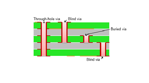
A printed circuit board includes a number of copper foil circuits, which are interlinked by vias. Via (through-hole, blind, buried, stacked, microvias) provides critical interlayer connections in high-density interconnection boards. Blind and buried vias increase the density of boards without adding size; hence, they are imperative for modern trends of miniaturization and high-speed signal transmission. These vias are plated with conductive materials, usually copper, so the electron flow can happen without much effort. Although advanced via types, like stacked vias, cost more, they save up much space and significantly improve routing capacity.
