Understanding ENEPIG in PCB Manufacturing
ENEPIG is a high-performance PCB finish with nickel, palladium, and gold layers, offering superior solderability, corrosion resistance, and wire bonding for critical industries like aerospace and telecom.
Printed Circuit Boards form the backbone of modern electronics, right from mass consumer gadgets to critical systems in space. As electronic devices forge ahead with developments, the need for reliable and efficient PCB surface finishes has become a general requirement. Among the different options for the same, ENEPIG stands out, which goes by the name of Electroless Nickel Electroless Palladium Immersion Gold, owing to its exemplary performance attributes. The article is a how-to guide discussing what makes ENEPIG better for high-performance PCBs and compares it to other finishes such as ENIG, which stands for Electroless Nickel Immersion Gold.
What is ENEPIG?
ENEPIG is a multi-layer, complicated coating on PCBs. It allows for superior corrosion resistance, solderability, and capabilities of wire bonding. The three layers are deposited one after another on top of each other, namely nickel, palladium, and gold. Each of these performs a different function:
Nickel Layer: Laid electrolessly, as the first layer, nickel prevents the diffusion of copper and provides a sound base for the succeeding layers. The thickness normally ranges from 3 to 6 microns.
Palladium Layer: Palladium is a thin layer laid over the nickel layer, with a thickness ranging between 0.05 to 0.2 microns. It exhibits outstanding resistance to corrosion and protects the nickel layer against oxidation and prepares it for the deposition of gold.
Gold Layer: Outermost 0.03 to 0.1 micron immersed plated layer that prevents oxidation and allows for very good solderability for attaching components onto the board.
How ENEPIG Works
The ENEPIG manufacturing process is primarily a process called electroless deposition, which consists of no external power source. In fact, this method is inherently robust and reliable and ensures that the layer thickness is uniform over the PCB. The major stages of the process involved in manufacturing for ENEPIG are mentioned below:
Copper Activation: One of the most important steps in the adhesive properties of the nickel layer is the treatment of the copper surface. Cleaning or etching of the copper removes contaminants and oxides, thus providing an optimum substrate for plating.
Electroless Nickel Plating: Deposit a layer of nickel on the activated copper. Such a layer would serve as a barrier to prevent copper migration and offer a stable substrate for deposition of the palladium and gold layers.
Electroless Palladium Plating: The second layer is palladium, a corrosion-resistant metal. This layer is very crucial, as it enhances finish durability and proper adhesion of gold effectively.
Gold Immersion Plating: The gold improves solderability by preventing oxidation with the additional gold layer. It is used to coat PCBs reliably to enable assembly and long-term performance.
ENEPIG Advantages
Improved Solderability: The gold layer in ENEPIG allows for better solderability and thus finds applications in high-reliability markets where consistent and strong solder joints are required.
Excellent Corrosion Resistance: The corrosion resistance is radically improved with a palladium buffer layer protecting the nickel, thus assuring long life even in very harsh environments.
Improved Wire Bonding: ENEPIG is compatible with both gold and aluminum wire bonding, thus extending its applicability for a wide range of assembly requirements, from simple to very stringent, such as in aerospace and telecommunications.
Low Contact Resistivity: The multilayer composition of ENEPIG provides very low contact resistivity, hence extending its usage into RF and microwave applications where high-frequency performance is required.
Limitations of ENEPIG
While ENEPIG indeed boasts many advantages, it is by no means perfect:
Higher Cost: ENEPIG includes palladium, making it more expensive than simple finishes such as ENIG. Additional material and processing costs come with the extra layer.
Complex Manufacturing Process: ENEPIG is a multistep process that is painfully precise in nature. The increased lead times in manufacturing and added complexity versus single-layer finishes make it challenging.
Limited Availability: Not all manufacturers are equipped to make ENEPIG. This creates possible supply chain constraints of ENEPIG, particularly in smaller lots.
ENEPIG vs. ENIG
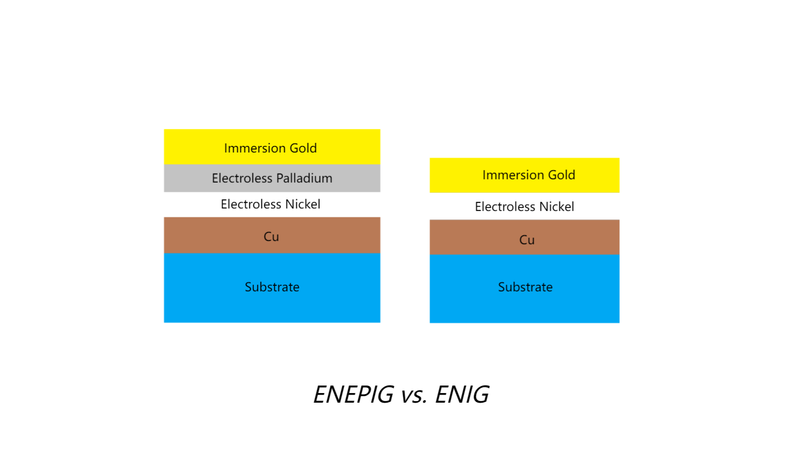
Cost: More expensive due to the added layer of palladium, while the general cost of ENIG is lower but will not give up much in performance for the more budget-conscious job.
Solderability: Both feature great solderability, but ENEPIG offers consistent and reliable joints due to its multi-layer structure.
Corrosion Resistance: ENEPIG certainly shows greater corrosion resistance with the inclusion of the palladium layer; ENIG may not be quite as robust in extreme conditions.
Wire Bonding: ENEPIG has the advantage of gold and aluminum wire bonding, but ENIG is confined to gold wires.
Applications of ENEPIG
High-Reliability Applications: In industries that have no margin for errors-aerospace, medical devices, and telecommunications-ENEPiG tops the list among all other metals.
Automotive Electronics: Since ENEPIG is capable of withstanding immense pressure, this material is suitable for ADAS and engine control units.
RF and Microwave Circuits: ENEPIG, with its ultra-low contact resistance, is especially suited for very high-frequency applications because it ensures good data transmission in telecom infrastructure.
Conclusion
ENEPIG represents the epitome of surface technology on printed circuit boards. Its unrivaled reliability, performance, and versatility bestow special status upon it among other finishes. Higher costs and manufacturing complexity notwithstanding, its advantages often justify the investment required, especially for high-stakes applications. ENEPIG is an optimum solution for industries requiring strong and reliable PCBs, enhancing functionality and the life expectancy of electronic assemblies. Being one of the most popular choices among high-tier surface finishes, ENEPIG continues to raise the bar high in the production of PCBs and, therefore, becomes a decent option to consider for your next high-performance project.
Hot Tags:
Contact us

If you can't find what you're looking for, please contact us.
Article
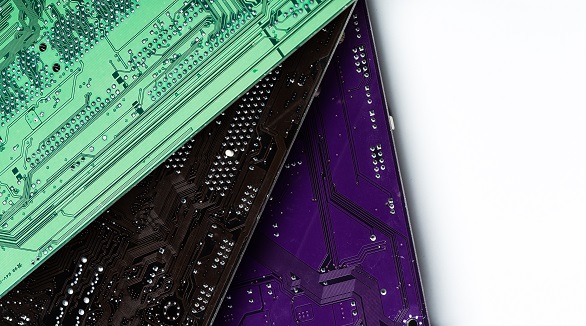
PCBs (Printed Circuit Boards) are fundamental in electronics, composed of multiple layers like silkscreen, soldermask, copper, and substrate, chosen for specific electrical functions.
The trend towards lead-free PCB manufacturing comes due to the EU's ROHS directive, which requires compliance to the limits on the content of lead. Compliance with lead-free is achieved by different surface finishes such as ENIG, ImAg, ImSn, and OSP—all with their different pros and cons. This paper compares these finishes to help choose the best for specific PCB applications.
The article insinuates the need for Organic Solderability Preservatives on printed circuit boards. OSP can adsorb onto the copper surface to prevent oxidation and moisture and can easily get washed out by soldering. It is easy to manufacture an OSP, which is environmentally friendly and not expensive, thus becoming one of the most popular surface finishes today.