- Products & Capabilities

- Simulation Design & EDA

- About
- Resources
Understanding Gold Plating in PCB Manufacturing


Gold plating in PCB manufacturing increases electrical properties, durability, and corrosion resistance, ideal for high-reliability applications. Types include ENIG (common, flat, solderable) and ENG (thicker, durable).
Gold plating in PCB manufacturing refers to the process of depositing a thin layer of gold on the surface of a printed circuit board, mainly above the copper pads and traces. This enhances the electrical properties of a PCB, durability, and corrosion resistance. Plating by gold is generally used in high-reliability applications that demand superior performance and long-term reliability.
Types of Gold Plating Used in PCBs
There are primarily two variants of gold plating utilized in the field of PCBs: Electroless Nickel Immersion Gold and Electrolytic Nickel Gold.
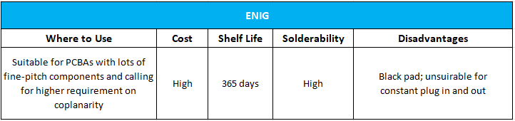
1. Electroless Nickel Immersion Gold (ENIG)
ENIG is the most common form of gold plating used during the production of PCBs. It consists of two layers: an undercoat made of electroless nickel and overlaying that, a thin layer of immersion gold.
Process:
The layering involves the following processes:
Electroless Nickel Plating: Nickel is chemically deposited onto the copper pads, making a very thin barrier layer for copper protection and giving a good surface to the gold layer.
Immersion Gold Plating: Immersion process chemical deposition of a thin layer of gold over the nickel layer; protects the nickel, and at the same time provides a solderable surface.
Advantages
Flat Surface: ENIG provides a very good flat surface for fine-pitch components.
Excellent Solderability: A gold surface offers very good solderability. The possibility of defects due to poor solderability at the time of assembly is reduced.
Oxidation Resistance: Due to the gold layer, it neither oxidizes nor corrodes. It will provide more reliability in the long run.
Durability: The layer of nickel gives good mechanical strength.
Disadvantage
Cost: This process is more costly compared with some other finishes due to the price of the gold.
Black Pad Syndrome: Potential failure mode where the nickel layer corrodes and through which solderability degrades.
2. Electrolytic Nickel Gold (ENG)
The Electrolytic Nickel Gold is, in fact a method of applying nickel and gold layers through an electrolytic process by dipping the printed circuit board into a common electrolytic bath and running an electric current that deposits the metals onto the boards.
Process:
Electrolytic Nickel Plating: The copper pads are electroplated with a layer of nickel.
Electrolytic Gold Plating: A thicker layer of gold is electroplated over the nickel layer.
Advantages
Thicker Gold Layer: Good for resisting wear and, therefore, is suitable for edge connectors and high-contact areas.
Strong Adhesion: The process of electrolytic deposition offers very good adhesion to the gold layer.
Long Shelf Life: The increased thickness of the gold layer prolongs the durability and shelf life of the PCB.
Disadvantages
Complex Process: It is more involved in its electrolytic process and requires more controls.
Higher Cost: The thicker layer results in higher costs.
Applications of Gold Plating in PCBs
Gold plating applies on the PCB to serve various high-performance applications reliably:
Military and Aerospace: The gold plating satisfies the needs for high reliability where one cannot afford to experience any failure.
Medical Devices: Devices that require biocompatibility and are intended for very reliable service.
Telecommunication: High-frequency and high-speed circuit boards.
Consumer Electronics: High-end products with high requirements on performance and lifespan.
Automotive: For safety-critical and control systems.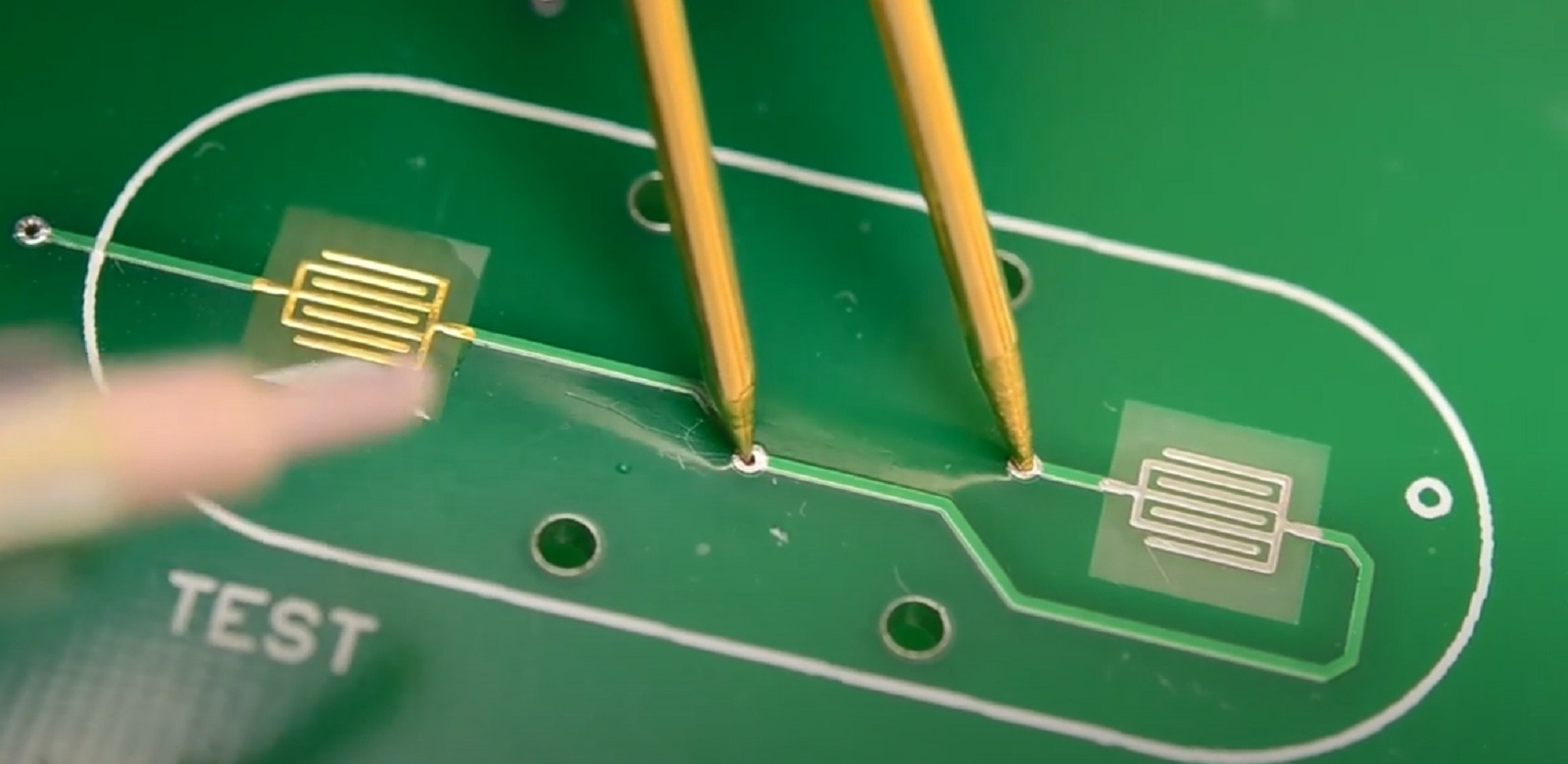
Advantages of Gold Plating
The advantages of gold plating in the manufacture of PCBs are numerous:
Improved Electrical Performance: A good conductor, gold enhances signal integrity and reduces resistive losses.
Superb Solderability: Its solderability ensures strong, reliable solder joints.
Corrosion Resistance: The element gold is resistant to oxidation and corrosion, further adding to the durability and life expectancy of a PCB.
Mechanical Strength: Extra mechanical strength is provided by a layer of nickel underneath.
Life Cycle: With the long-lasting life of gold-plating, it gives long life cycles to a PCB in intense atmospheric conditions.
Considerations for Gold Plating
Gold plating in printed circuit board manufacturing includes a number of factors that have to be considered:
Cost vs. Benefit: Consider the cost of gold plating in light of the benefit derived from it.
Application Requirements: Consider the demands of the environment in which the assembly will function, including any exposure to temperature extremes, chemicals, mechanical stress, and whether it requires high reliability.
Type of Gold Plating: Choose between ENIG and ENG based on particular needs that may present themselves with your PCB design.
Possible Issues: Be aware of the probable black pad syndrome, among other issues that might arise; do the necessary quality control.
Conclusion
Some of the major advantages of gold plating in PCB manufacturing include improved electrical performance, better solderability, and higher corrosion resistance. Knowledge of ENIG and ENG types of gold plating, along with their relative advantages and disadvantages, enables designers and manufacturers to make optimal selections in conformance with their needs for a particular application. Since gold plating is more expensive, it logically sees its widest usage in high-reliability applications of all varieties, hence becoming important in today's electronics manufacturing.
Hot Tags:

Contact us

If you can't find what you're looking for, please contact us.
Article
Selecting the right PCB surface finish, from options like HASL, ENIG, ENEPIG, and OSP, is crucial for preventing oxidation, ensuring solderability, and meeting reliability standards.
 2024/08/07
The trend towards lead-free PCB manufacturing comes due to the EU's ROHS directive, which requires compliance to the limits on the content of lead. Compliance with lead-free is achieved by different surface finishes such as ENIG, ImAg, ImSn, and OSP—all with their different pros and cons. This paper compares these finishes to help choose the best for specific PCB applications.
2024/07/29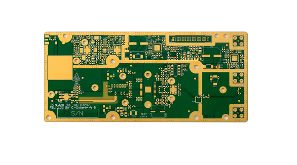
The article insinuates the need for Organic Solderability Preservatives on printed circuit boards. OSP can adsorb onto the copper surface to prevent oxidation and moisture and can easily get washed out by soldering. It is easy to manufacture an OSP, which is environmentally friendly and not expensive, thus becoming one of the most popular surface finishes today.
2024/07/25