Understanding PCB Tab
PCB tabs ensure mechanical stability and easy assembly. They facilitate fabrication by retaining panel stiffness, holding boards, and aiding in depaneling, optimizing manufacturing efficiency and quality.
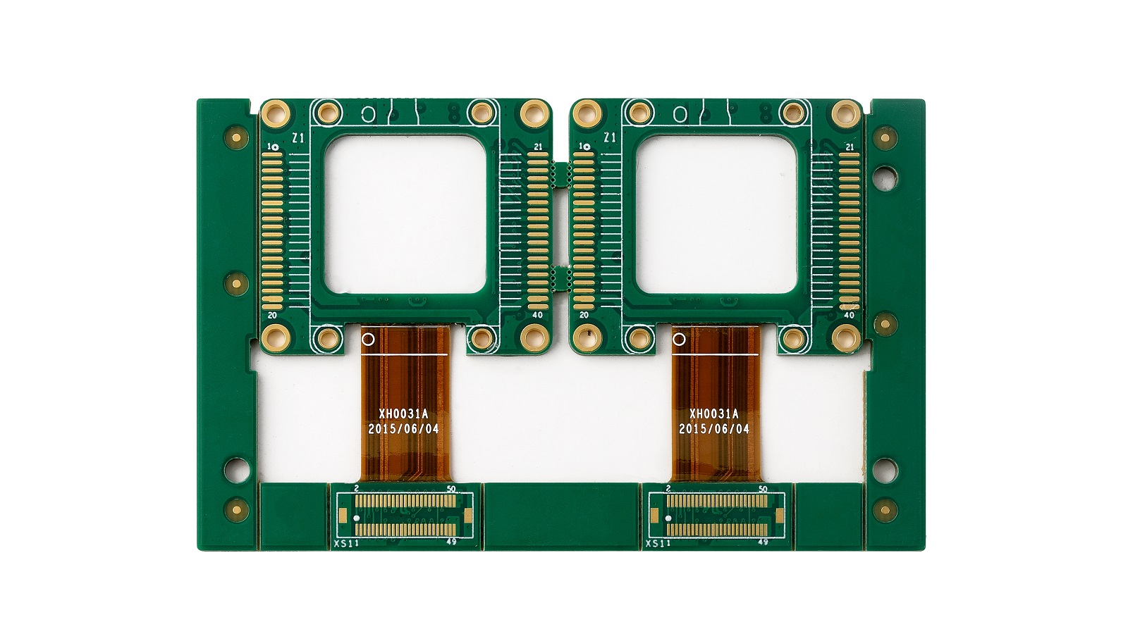
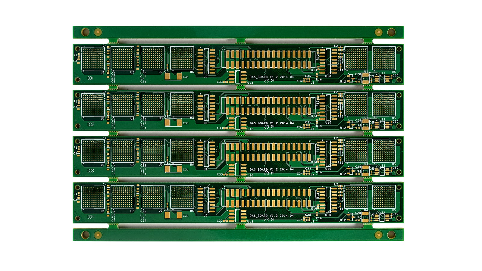
A PCB Tab can also be called a printed circuit board tab, which is an extension of the material from the PCB, generally placed strategically for mechanical stability, efficient production, and easy assembly. Tabs should be of a size that can easily be broken off after the board has gone through several production stages. This article is going to overview tabs on a PCB, ranging from the purpose, design considerations, placement of tabs on the board to fabrication and assembly considerations.
Functions of PCB Tabs
Panel Stiffness Retention
During manufacturing, many PCBs are fabricated on one large panel for effective production to avoid any handling issues. PCB tabs keep these panels stiff during fabrication. Tabs bridge the gaps between boards to avoid warping and damage throughout shipping and handling. This rigidity facilitates easier loading and transfer through automated machinery.
Holding Boards in Panel
PCB tabs serve to hold individual boards securely in place within the panel and prevent movement or premature fallout. A well-designed tab is strong enough to resist machine insertion forces and accelerations without tearing and releasing the boards.
Typical PCB Tab Design
Though specific parameters may vary between manufacturers, typical design specifications for PCB tabs include:
Width: 0.2" to 0.4" (5mm to 10mm)
Length: 0.4" to 1.2" (10mm to 30mm+); Corner Radius: 0.06" (1.5mm); Pattern: Repeating groups of tabs along panel edges.
These dimensions offer a great compromise between strength and space efficiency. These are robust tabs that support fabrication stresses while maintaining board positioning and panel rigidity.
PCB Panel Tabbing Guidelines
For proper functionality, there are design guidelines that a PCB panel tab must adhere to:
Placement Frequency: Tabs to be placed at periodic spacing along the edges in intervals of 3" to 5" (75mm to 125mm).
Location: Tabs shall be placed at corners and along potential separation lines within the panel.
Stress Consideration: High Router Force Areas may require closer Tab Spacing.
Special Shapes: Radial tabs can hold circular boards effectively.
Size and Thickness: Larger or thicker boards may need bigger, stronger tabs.
Precision Cutting: The width of the tabs should correspond to the width of the router blade for neat cuts.
Tab placement typically results from collaboration between designers and fabrication houses based on particular panel size, shape, and available equipment capabilities.
Alternatives to Full Tabbing
There are some instances where full tabbing on all edges of panels may not be beneficial or realistic to offer. These include:
Low Tab Density
A limited number of intermittent tabs can offer positioning without any loss in panel rigidity for less complex boards.
Breakaway Tabs and Score Lines
Delicate, fracturable tabs or score lines provide break points for easy removal and eliminate the necessity for heavy-duty tabbing.
Tooling Holes
Round tooling holes, in conjunction with partial tabs, can also hold panel alignment.
No Tabs
Boards that are designed for smaller panel sizes can be shipped without tabs, thereby eliminating manufacturing steps.
Specialty Shielding
For metal-shielded boards, plated tabs can short out shielding. Insulating sections or adhesives are alternatives.
Castellated Edges
Interleaved castellations along edges can hold position - eliminating the need for traditional tabs.
Impact of Tabs on Fabrication
PCB tabs affect several fabrication steps:
Panel Layout
Tab size and spacing determine how many boards can fit on a panel as larger tabs reduce panel utilization.
Imaging
Tabs reduce tooling image sizes, closer spacing allows smaller tools.
Stress Absorption
Tabs absorb shear handling and drill forces, relieving the boards from much of the internal stress that might be generated.
Drilling
Drill bits must penetrate tabs cleanly without cracking and residuals.
Routing
The tabs are to be cut precisely without tearing or leaving burrs.
Masking
Liquid photoimageable solder masks must coat the edges of tabs without bridging.
Testing
Tabs should be avoided in the design of fixture contacts for in-circuit testing, and probing may affect the grounding of tabs.
Assembly
Tabs should not obstruct components, and their location should be planned in pick-and-place programs.
Depaneling PCBs
After fabrication and assembly, the tabs are normally removed by depaneling the PCB. The methods used include:
Tab Routing
A final routing passes slices tabs flush with board edges in one action.
Tab Punching
Pneumatic punch dies snap off tabs, leaving smooth edges.
Break Tabs
Operators manually break off thin breakaway tabs in the routing process.
Retaining Tabs
Sometimes, tabs can also be left to remain on the board and only those which are not needed are removed.
Conclusion
Tabs in the PCBs play a vital role in the process of panelization and fabrication of printed circuit boards. Effectively designed tabs positively affect the yield of manufacturing and the quality while reducing impact on space and cost. Tabs, when integrated along with PCB fabricators, can be a very valuable aspect of panelized board production. At PCBX, we specialized in optimizing PCB design and manufacturing to ensure the best possible outcomes for your electronic product. For further insights or assistance, reach out to our professional team today.
Hot Tags:
Contact us

If you can't find what you're looking for, please contact us.
Article
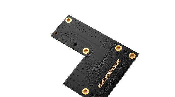
Plated-through slots (PTS) in PCBs are copper-plated apertures for electrical connectivity, offering space optimization, reduced soldering voids, and improved surface use.
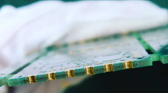
Plated half-holes allow for high-density, miniaturized electronic connections with ease of soldering and efficient board integration—two of the basic needs of modern PCB designs and applications today, such as WiFi modules.
The article is developed concerning the breakthrough of integrated circuits and the need for custom PCBs in some electronic products. It enumerates ten golden rules in conducting PCB layout design and manufacturing: grid selection, routing, power layers, component placement, panel duplication, component value combination, frequent DRC, flexible silkscreen use, decoupling capacitors, and pre-production parameter checks. These rules provide for the optimum design and manufacturing of a PCB.

