Understanding Selective Soldering in Electronics Manufacturing
Selective soldering offers precision and efficiency for complex PCB assemblies, targeting specific areas with improved quality, cost-effectiveness, and flexibility, overcoming limitations of wave soldering.
The assemblies of printed circuit boards today are very complex, mostly because surface mount components are mounted on both sides of the board. In turn, soldering methods and techniques have to be improved continuously. Wave soldering, normally common, does not suffice for such intricate boards. It is at this juncture that the need for selective soldering sets in: precision, efficiency, and reliability for through-hole components in today's complex assemblies. Selective soldering allows the automation of the soldering process by facing most of the challenges and keeping quality and productivity at their optimum.
Fundamentals of Selective Soldering
The name itself suggests that in selective soldering, selected or specific components are soldered on a PCB. Unlike in wave soldering, where the entire board is swept over a wave of molten solder, in selective soldering, the board receives material in very precise areas. Thus, the process starts by generating a program from a PCB image where paths are defined regarding the placement of flux and solder.
There are three critical steps common to wave soldering and selective soldering: flux application, preheating, and soldering. In practice, these vary significantly. Flux is only applied to the areas that need solder, thereby limiting the exposure of the board and reducing the risk of thermal shock. The preheat stage is significant mainly because it raises the temperature of the board so that once solder is introduced, flow occurs and joints can be set. In selective soldering, there is unmatched precision since soldering takes place as individual connections are exposed to molten solder in sequence.
Why Selective Soldering is Preferred

Selective soldering has found its place in the industry and finds increasing application because of a host of advantages over the conventional methods, especially in those assemblies where the conventional techniques falter. This includes:
Precision and Control
It enables selective soldering to accurately specify which areas of the PCB should be soldered, minimizing the chances of bridging and heat damage to sensitive areas. Each solder joint can be programmed individually for optimum quality.
Improved Quality
High-purity nitrogen used in the process prevents solder oxidation, which means a decrease in defects and high-quality joints. Nitrogen gas provides a controlled environment that keeps the oxidizing agents away, which preserves the integrity of the solder.
Flexibility for Complex Designs
The most valuable benefits of selective soldering include the preciseness of targeting needed for such dense PCB layouts with minimal clearance between the components. This minimizes the interference risk of SMT pads and its components, which are generally regarded as the deficiencies in wave soldering.
Cost Effectiveness
While the initial setup cost of selective soldering equipment is expensive, the returns on investment through reduced defects and fewer labor costs with improved throughput take little time. Additionally, the automation of the process reduces lead times and overall manufacturing costs.
Considerations and Components of Selective Soldering
Understanding the consideration and components of selective soldering will help a great deal in enhancing its deployment into the manufacturing process.
PCB Size and Machine Configuration
They start from small, single-assembly setups to larger inline systems. The selection of the machine should allow consideration of the maximum PCB size the process will need to handle. Flexibility can be implemented using either dual conveyors or additional solder pots to increase throughput.
Floor Space and Maintenance
Selection would depend on the availability of space; small operations may allow compact machines that may be operated without handling systems. Larger ones would involve handling systems to control the machines. From a maintenance point of view, in particular for solder pot technology, machines with electromagnetic pumps seem to need less maintenance and offer steady high-precision soldering.
Solder Type and Solder Pots
The solder alloy types can be accommodated for selective soldering. In many applications, lead-free solder is applied because of regulatory standards. Temperature control is very important and will depend on the application; a typical range could be between 270°C and 300°C, depending on the desired characteristics of the flow. Advanced machines could have multiple solder pots, each of which allows for different alloys or nozzle sizes in applications requiring versatility.
Nozzles and Nitrogen Supply
There are different shapes and sizes of nozzles, which are basically meant for accessing narrow areas of soldering. Nitrogen supply from sources like pressurized bottles and tanks and on-site generation of nitrogen creates an oxide-free environment for the solder. The purity of nitrogen has to be maintained at 99.999% to avoid any dross formation which might affect the soldering process in case of smaller nozzles.
Flux and Pre-heating
Fluxes in selective soldering are basically of the low-solids/no-clean type and support minimal residue. Effective preheating by way of convection or infrared, with closed-loop control, ensures fill of solder and avoids thermal shock. Proper application of flux and its preheating ensure strong and reliable joints besides clean and efficient operations.
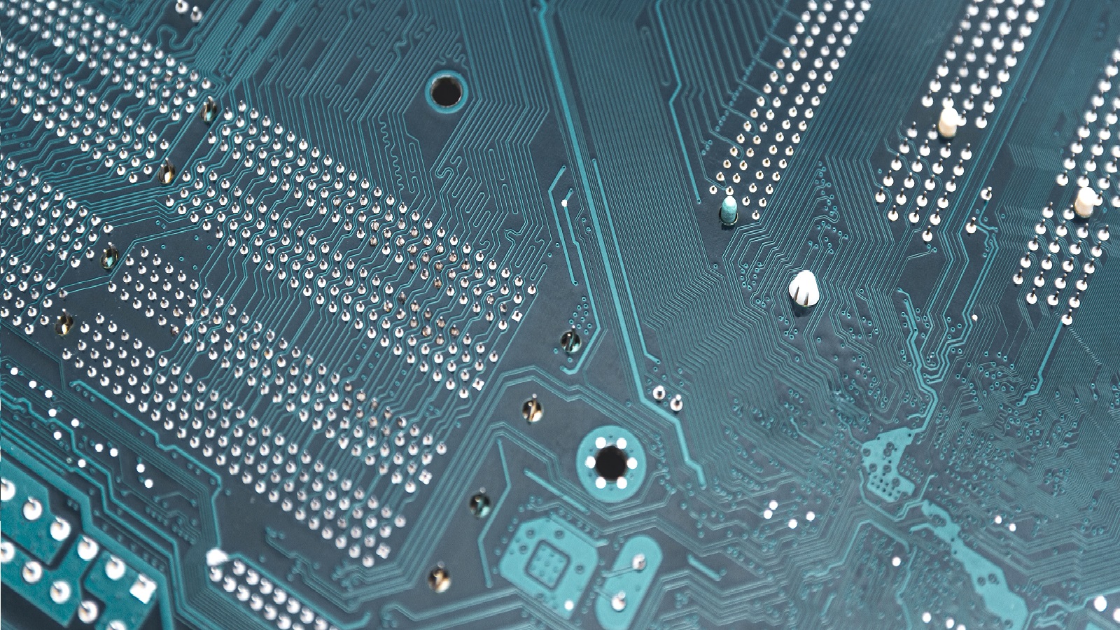
PCB Handling And Machine Options
Inline systems, by contrast, need effective board handling solutions to achieve large-scale operations. The machines can also be specified with automated features like nozzle cleaning, solder level checking, and compensation for warp in order to extend repeatability and simplify processes. Some options further increase the precision and reduce the complexity of operation.
Conclusion
Selective soldering has become a redefinition in the soldering process for PCB manufacturing, especially in designs where precision and control need to be in place to avoid defects and ensure quality. Automation in what had been a manual process fraught with the potential for error serves to enhance both reliability and efficiency for electronic assemblies.
For subcontract manufacturers, often denied any influence over PCB design, it is extremely valuable to have access to the accurate and stable solder waves characteristic of selective soldering, especially with the close clearances that are often encountered. The investment in selective soldering equipment is very significant; however, the cost benefits can be realized quickly through improved product quality, higher yields, and reduced manufacturing time and cost.
In this respect, selective soldering is representative of a qualitatively new answer to the needs that arise in the process of the production of present-day electronics since it offers the qualities of flexibility and accuracy through which it contributes to increasing the quality and productivity of the process as a whole, making it an indispensable tool in the arsenal of every competitive manufacturer of electronic products.
Hot Tags:
Contact us

If you can't find what you're looking for, please contact us.
Article
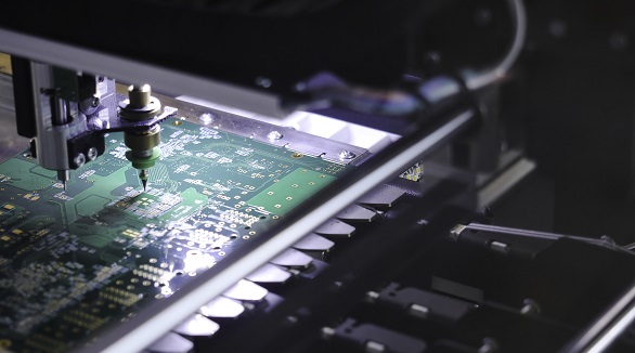
Reflow soldering is vital for PCB assembly but faces challenges like solder bridging, tombstoning, and voiding. Effective solutions include optimized stencil design, thermal profiling, and precise component placement.
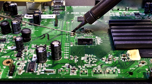
SMD soldering mounts small components on the PCB surface for compact, automated designs but has high setup costs and repair challenges. DIP soldering uses through-hole components for robust, easily repairable, lower-volume applications.
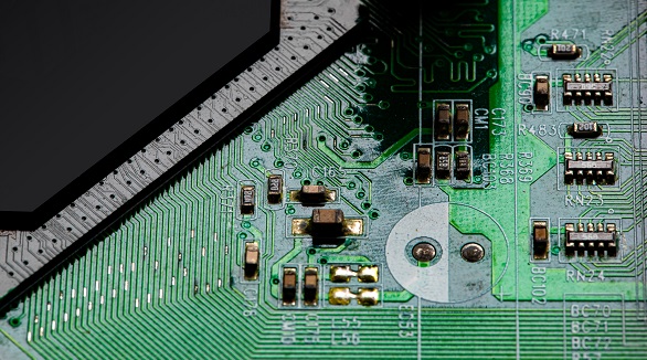
Solder mask, or solder resist, is the polymer layer on PCBs that protects against oxidation, short circuits, and solder bridges. Types include LPI, dry film, and epoxy, chosen based on design, application, and cost.