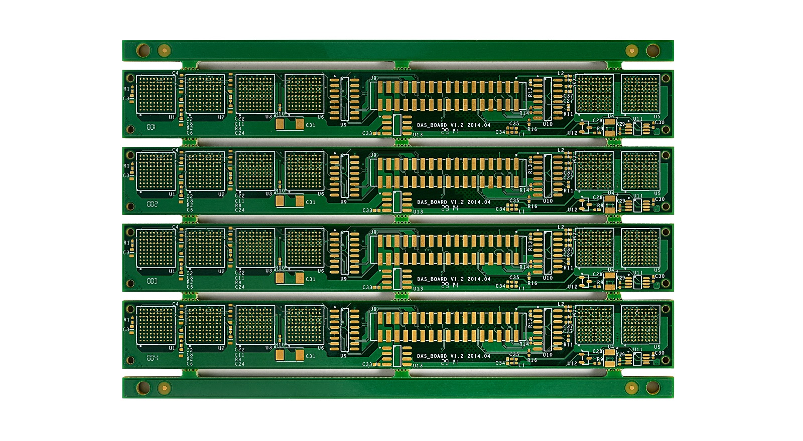
What is Any Layer HDI PCB?
Any Layer HDI PCBs optimize space and performance with high-density connections, enhancing electronics across industries with reliable, cost-effective solutions.
With the present evolving era of electronics, the demand for equipment not only smaller but with increased power continues to increase day by day. With this demand in view, technologies of printed circuit board (PCB) development continue to advance enormously, e.g., the invention of High-Density Interconnect (HDI) PCBs. The foremost innovation of the current age is the "Any Layer" HDI PCB design, an assembly that discovers an ideal combination of the small size factor and the function factor. In this comprehensive guide, we at PCBX, professionals in the area of PCB design and content marketing, explain the intricacies of Any Layer HDI PCBs, their benefits, manufacturing process, and applications across industries.
PCBs can be found in various configurations like single-layer, multilayer, and flex circuits to support various electronic applications. HDI PCBs differ in that they can accommodate a higher number of components compared to normal PCBs. This is achieved through complex techniques like using multiple layers, trace widths which are thinner, and via-in-pad designs, all of which contribute to higher signal quality, reduced power usage, and an overall improvement in electrical performance.
Any Layer HDI PCBs are a top-of-the-range variation in this model. As opposed to regular PCBs with their limited interconnection, Any Layer HDI PCBs provide designers with the capability to connect any layer with microvias, blind vias, and buried vias. This unconstrained interconnectability allows designers to create efficient and complex circuits, which could lead to developing compact electronic products without compromising their functionality.
Manufacturing Process of Any Layer HDI PCBs
Designing Any Layer HDI PCBs is a step-by-step process of cautious measures with a focus on accuracy and dependability:
Layer Construction: This begins by combining and putting more than one layer of copper foil and dielectric material together. All of them are stuck together by a compression and lamination technique to form a rigid shape.
Laser Drilling for Vias: In contrast to mechanical drilling for traditional PCBs, laser is used to drill tiny microvias. Such precise drilling facilitates the integration of blind and buried vias that are necessary for efficient inter-layer connections without applying through-holes that go straight through the full board thickness.
Plating and Etching: Electroless plating is used for the deposition of thin layers of conductive material in the microvias to establish uniform electrical contacts. Then comes photolithographic imaging and etching to define the desired circuit patterns on each layer.
Lamination: The boards are lamination in sequence, a technique of incremental addition of the board through layers. Different stacking configurations such as 1+N+1, 2+N+2, or even intricate ones are employed depending upon design requirements. It is a crucial step to include routing density as well as create complex designs.
Advantages of Any Layer HDI PCBs
Better Signal Integrity: By incorporating technologies such as blind vias and via-in-pad, HDI boards leave space for components to be placed closer to one another, keeping signal track lengths as small as possible. The elimination of stub vi locations eliminates reflection, greatly enhancing signal quality and integrity.
Efficient Use of Space: The reduced size of Any Layer HDI boards allows for more efficient use of space by having more components in less space, making them ideal for modern, mobile electronic products.
Improved Reliability: HDI PCBs employ microvias, which are more reliable than standard through-hole vias. Being small in size and having a very precise positioning, they result in a strong and reliable circuit structure, with less possibility of failure.
Cost-Effective Production: Regardless of the advanced technologies utilized, Any Layer HDI PCBs are likely to consist of fewer layers than multilayer boards, hence saving production costs. The cost-effectiveness is realized without sacrificing performance, which makes such boards a cost-effective solution for the majority of applications.
Applications in Various Industries
The versatility and efficiency of Any Layer HDI PCBs make them a well-known choice in various high-performance devices in a variety of industries:
Consumer Electronics: Consumer electronics such as smart phones, tablets, and wearables significantly utilize the miniaturized design and high-end capabilities offered by Any Layer HDI PCBs. These boards offer space for devices to be minimized without losing capabilities.
Medical Technology: The precision and reliability of HDI PCBs have them as a component of advanced medical equipment, such as portable diagnostic equipment and miniaturized cameras for high-quality imaging of internal organs and tissues.
Automotive and Aerospace: With newer cars and aerospace technology demanding small, reliable electronics, HDI PCBs provide the basis for advanced infotainment systems, safety features, and connectivity features, enhancing performance and lifespan.
Military and Industrial Applications: Under conditions demanding high reliability and performance in harsh environments, HDI PCBs excel. They are used in military equipment and industrial IoT devices where longevity and miniaturization are paramount.
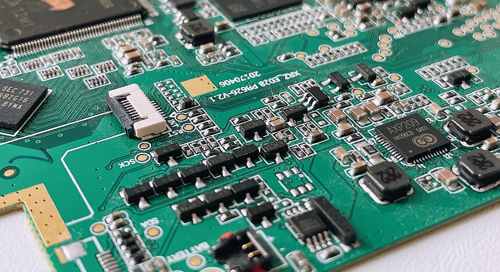
The advent of Any Layer HDI PCBs is a revolutionary advance in PCB technology that, in a direct manner, responds to the demands for space-saving, powerful, and efficient electronic solutions. PCBX is leading this change in technology and is delighted to be utilizing its expertise to offer cutting-edge solutions for the needs of today's industry. As electronic equipment becomes more diminutive in size but expansive in capability, the role of Any Layer HDI PCBs is going to stay fundamental to the future of electronics. This technology not only serves the current industry's demands, but it provides a basis for what is to come in the future, ensuring electronic products keep becoming more advanced and able.
Hot Tags:
Contact us

If you can't find what you're looking for, please contact us.
Article
High-frequency PCBs are crucial for fast, reliable tech, enhancing performance in telecoms, aerospace, and more with advanced materials and precise designs.
In-Circuit Testing ensures PCB reliability by verifying component integrity and connections, with advantages in accuracy and coverage, but high setup costs.
High-frequency circuits face thermal noise challenges. Minimizing resistors and optimizing circuit design can improve performance and reliability.

