- Products & Capabilities

- About
- Resources
What is DIP?


DIP is a basic, cost-effective IC package with dual-row pins, offering ease of use and reliability but taking more PCB space. It's ideal for prototyping and durable applications.
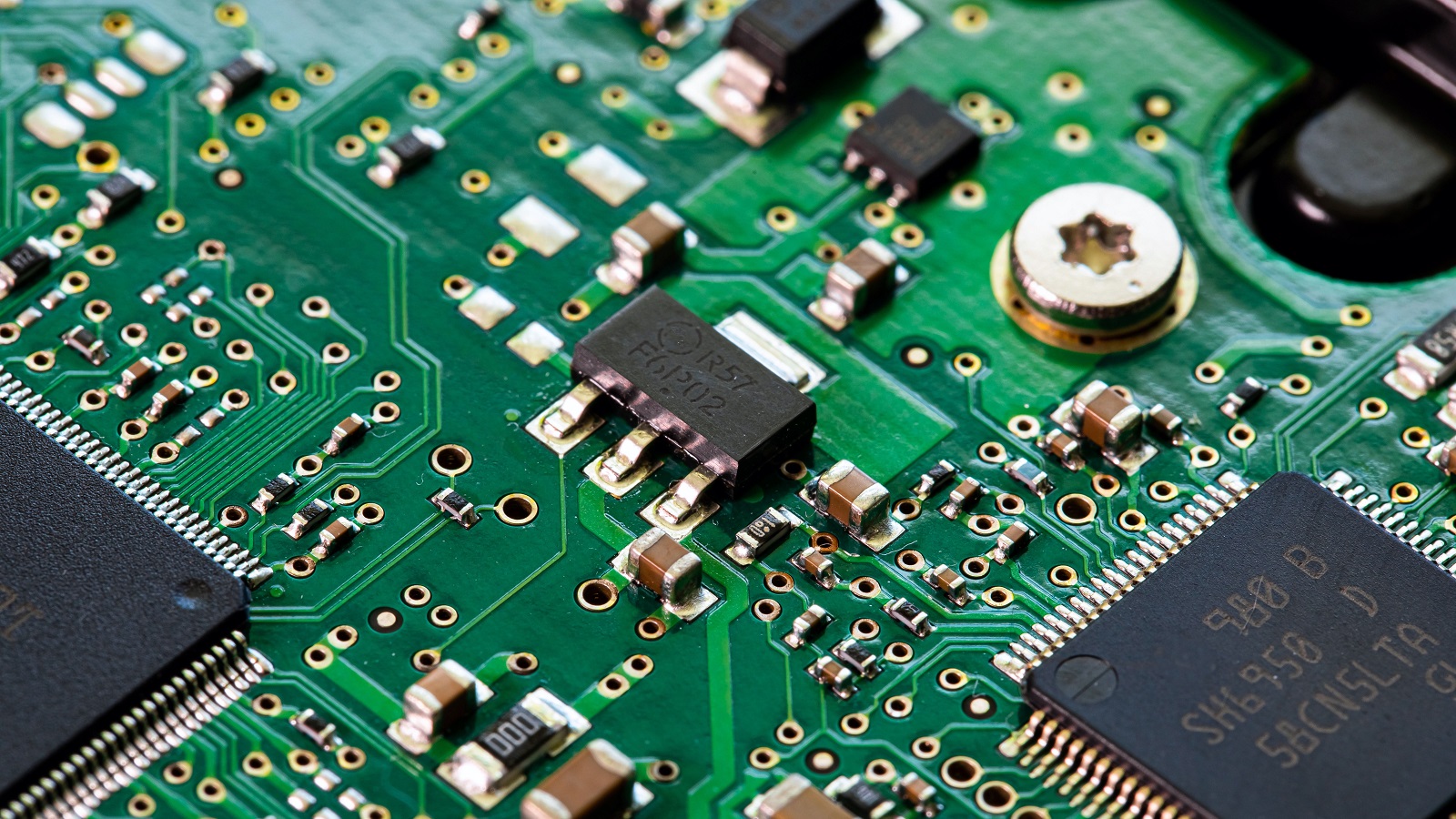
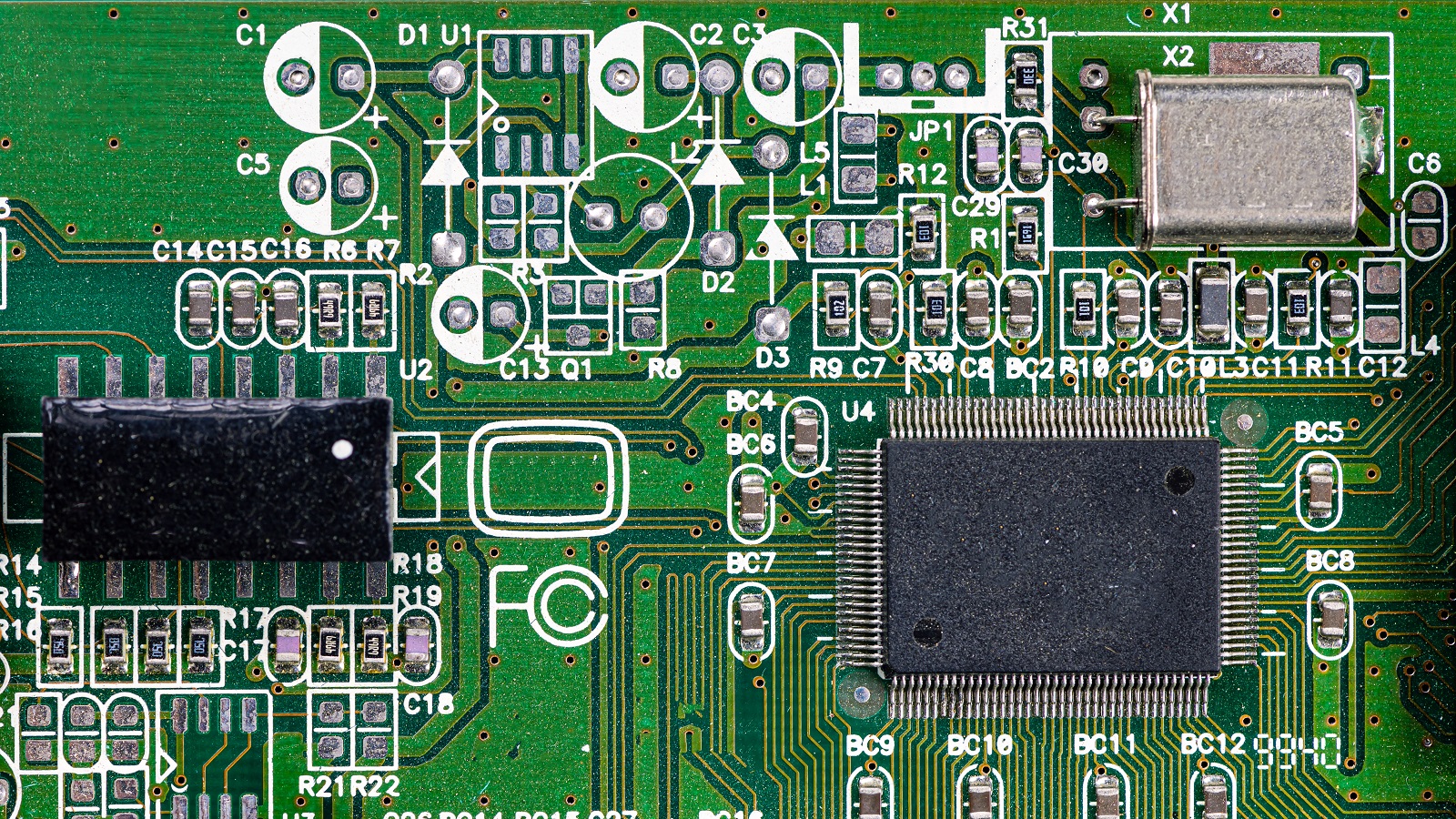
In this highly interconnected electronic world today, Dual Inline Package, or in its abbreviation form, DIP, is the basic, standard method of package for integrated circuits to be installed onto a PCB. It includes a symmetrical package with two rows of parallel pins usually directly connected with the PCB through soldering, or inserted into a compatible socket for more rugged and durable connection. This overview will outline the structure, features, advantages, and disadvantages of DIP and their applications to help in achieving a good understanding of its role in electronic circuit design.
Structure and Features of DIP
The DIP construction is robust yet simple. This is one of those cases where a silicon die is enclosed in a generally rectangular body made from epoxy resin, say, to which the pins are attached. These pins, usually made of copper but with a plating of gold, tin, or silver, form what gives this package type its name: dual-inline.
Main structural elements
Pin Count and Pitch: DIPs are designated by their number of pins: DIP8, DIP16, etc., which basically means the number of pins on the two rows. Conventional pin pitch is 2.54 mm or 0.1 inches to ensure compatibility with all types of applications around the world, though it does vary depending on specific uses.
Lead Frame and Silicon Die: The lead frame provides mechanical support for the silicon die while conducting electrical signals through the gold wire bonds. This configuration enables the internal circuitry to communicate with external components.
Protective Overmold: The entire assembly is encapsulated in a polymer mold, which protects against environmental damage, enhances thermal performance, and maintains reliability by preventing moisture ingression.
DIP: Advantages and Disadvantages
Advantages
Low Cost and Simplicity: One of the key selling points of DIP is their relatively low cost, stemming from a relatively simple manufacturing process that is suited to high-volume production.
Ease of Installation and Handling: The package is very easy to work with, and the devices are well-suited for manual insertion and soldering, making them convenient for prototyping and educational purposes.
Thermal Efficiency: The most important advantages with DIPs are that they efficiently dissipate heat and reduce the chances of overheat, thereby prolonging the life cycle of the device.
Replaceability: They can be easily replaced or repaired, reducing the possibility of collateral damage to other surrounding parts when performing maintenance.
Disadvantages
Space Utilization: Since they have a dual row structure, DIPs take more space on the PCB, so they cannot be used for high-density or compact uses.
Susceptibility to Mechanical Stress: Although robust, DIPs are susceptible to bending or twisting which could cause it to mechanical failure.
Thermal Expansion Problems: Upon changes in temperature, the pins may expand or contract and long term may pose a risk of solder joint failure.
Installation of DIP Packages
For installing a DIP, holes are provided in the PCB at the places of the pins, to which the part is carefully soldered. Orientation is normally provided by an identification notch that aligns the part the correct way. Alternatively, the DIP sockets can be used to allow non-destructive removal for replacement or other purposes.
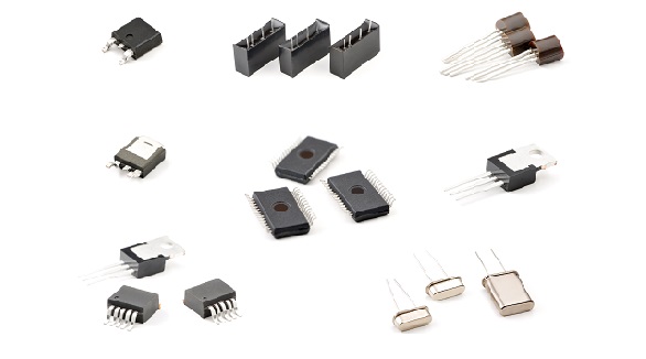
Variants and Types of DIP
The versatility of DIPs is manifested in the various types that fulfill certain needs, as shown below.
Plastic DIP (PDIP): This is the cheapest and finds the broadest application in general electronics.
Ceramic DIP (CDIP): It is improved to be resistant to moisture and extreme temperatures. Therefore, it is normally used in industrial and military applications.
Shrink and Skinny DIPs: These are variations that give a narrower footprint. These reduce area usage but retain functionality.
Quad Inline Package (QIP): It is an extension of the older DIP construction, adding more rows of pins for extra functionality in more complicated circuitry.
Applications and Evolution
DIP sees usage in a wide range of electronic components, from microprocessors to memory chips and other forms of ICs. The simplicity and reliability of DIP make it the standard in applications such as DIP switches, LED arrangements, strip displays, and seven-segment displays. While both SMT and SOP, with their entrances, have reduced the importance of DIP in certain fields, it is still remarkably relevant in the field of prototyping, learning platforms, and applications that require high durability and ease of assembly.
While SOP has reduced space and hence more compact, which is helpful in consumer electronics, DIP has its advantage when the application requires ease of handling and more strength in mechanical connections.
Conclusion
The Dual Inline Package has remained one of the stalwart members in the electronics industry, a component highly valued because of its reliability, ease of use, and cost-effectiveness. In as much as modern electronics are taking a grand leap, DIPs are still a formidable choice for many applications, especially where simplicity and toughness, such as in harsh environments, become necessary.
Hot Tags:

Contact us

If you can't find what you're looking for, please contact us.
Article
The ten essential electronic components are resistors, capacitors, diodes, zener diodes, inductors, varicap diodes, transistors, FETs, sensors, and transformers, each crucial for modern electronics design and functionality.
 2024/09/19
IC packaging is essential in electronics for protecting components, providing electrical connections, and managing heat. This tutorial explores its complexities, including its importance, various types like SMD, QFP, and BGA, and considerations for choosing the right package for specific applications. Proper IC packaging enhances PCB performance and reliability.
2024/09/12
Customers prefer one-stop PCBA service not only because of price transparency; it can save time and reduce labor costs with efficiency and professionalism in procurement and production.
2024/07/29