- Products & Capabilities

- Simulation Design & EDA

- About
- Resources
What is PCB Tombstone?


PCB tombstoning, caused by uneven soldering due to factors like pad design and component placement, disrupts circuits but can be mitigated through precise control and optimization.
In the accuracy-driven age of electronics manufacturing, printed circuit board (PCB) production is a process of fixing a broad spectrum of potential defects with critical impacts on the reliability and functionality of electronic devices. Among these defects is "tombstoning," an oddly named but disruptive defect that needs to be addressed by manufacturers to ensure product quality. As PCB manufacturing specialists at PCBX, we discuss this phenomenon in detail, taking into account its causes, effects, and prevention techniques.
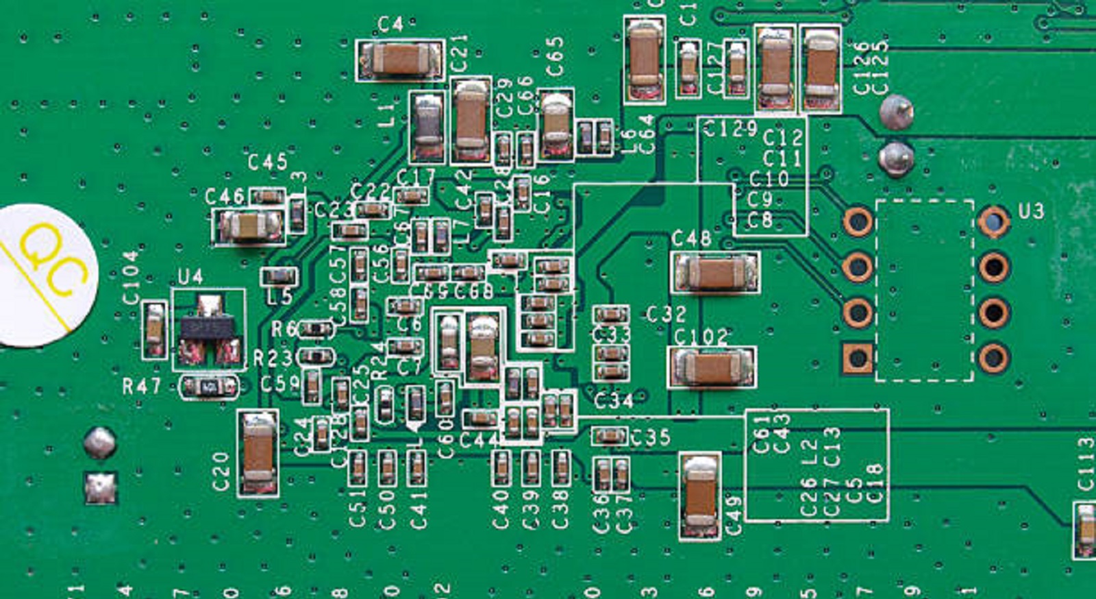
PCB tombstoning, a defect primarily observed in the reflow soldering process, is termed so due to the visual similarity it presents—where the top edge of an element such as a Mu
lti-layer Ceramic Capacitor (MLCC) protrudes from the PCB, resembling a tombstone. This protrusion occurs due to the non-uniform distribution of forces during soldering, particularly for smaller components due to their light weight and lower surface area.
Causes of Tombstoning
At the center of the tombstoning phenomenon is an imbalance in the wetting forces on the component's terminals. The main causes of this imbalance are presented as follows:
Asynchronous Melting of Solder Joints: One of the main reasons for tombstoning is the failure to achieve simultaneous melting of solder at both ends of the MLCC. This disparity typically occurs because of improper heat distribution during reflow, resulting in varying wetting forces that lift one end of the component.
Pad Design Discrepancies: Asymmetrical or ill-designed pads play a major role in tombstoning. If one pad is visibly larger or has a dissimilar shape compared to the other, it can hold more solder paste and dissipate heat differently, resulting in non-uniform solder adhesion.
Solder Paste Application Variations: Solder paste must be applied uniformly and consistently. Any variation, either by volume or composition through contamination, storage, or handling error, can influence solder joint quality and create unbalanced forces.
Incorrect Component Placement: Calculations of component placement on the PCB may lead to incomplete or improper contact with the solder pads. Even slight misalignments can amplify the effect of other contributing factors.
Consequences of Tombstoning
The process of tombstoning is more than a cosmetic defect; it has serious implications on the performance of electronic devices:
Electrical Discontinuity: The elevated region may result in an open circuit—halting part of the circuit and disrupting device function.
Higher Production Cost: The rework and repair work brought about by tombstoning generates higher cost of production and loss of yield, impacting profitability.
Reliability Failure: In the case of high reliability applications, e.g., aerospace and medical fields, tombstoning may hinder device reliability and safety and necessitate tight quality control.
Strategic Solutions for Preventing Tombstoning
Minimizing the risk of tombstoning is a function of design optimization, process refinement, and stringent quality standards. At PCBX, we give top priority to the following solutions for preventing tombstoning:
Ensure Simultaneous Solder Wetting: The reflow profile must be well controlled so that the solder paste melts at the same time at both ends of the component. This evenness minimizes the difference in surface tension that works to lift components.
Pad Design Optimization: Symmetry is vital. The pads must be symmetrical and appropriately sized to minimize the possibility of uneven solder distribution. End caps of MLCCs must overlap solder pads by at least 0.3 mm to provide good adhesion.
Provide Solder Paste Activity and Quality: Handle and store solder paste properly. Store at suggested temperatures (5-10°C), acclimatize to room temperature prior to use, and mix thoroughly to ensure even consistency. Any unused solder paste should be handled carefully to avoid contamination.
Component Cleanliness: Surface contamination of the MLCC should be avoided. Cleaning processes must be implemented by users and manufacturers to prevent residues that can affect solder wetting.
Take Advantage of Technology Improvements: Utilize new placement machines that have the capability of correcting X, Y, and rotation misalignment error in order to maintain correct placement and orientation of components.
Other Factors for Successful Implementation
Optimize Pad Space and Width: Keep minimum pad space but sufficient for the solder to cover it appropriately, while the remaining part of the length is usually not greater than 0.5 mm. The pad width also needs to be proportionally reduced based on the MLCC size.
Environmental Stability: Provide a stable ambient condition when applying solder paste to prevent localized environmental changes that may impact the soldering process.
Routine Process Review and Audits: Conduct regular process reviews and employ continuous improvement methods to establish and rectify potential causes of tombstoning.
PCB tombstoning is a major concern in electronics manufacturing, as it directly influences product quality and reliability. By understanding the driving forces of such a defect and applying strategic actions at design, process, and material control, its occurrence can be significantly relieved. At PCBX, our commitment to excellence and innovation ensures we provide the knowledge and solutions needed to overcome these kinds of manufacturing problems, enabling the creation of more reliable, cost-effective electronic assemblies. By employing knowledge-based practices and method-based precision, we not only minimize the likelihood of tombstoning but enhance overall manufacturing success and product performance as well.
Hot Tags:

Contact us

If you can't find what you're looking for, please contact us.
Article

Cold solder joints result from improper soldering, impacting PCB performance. Detection and prevention via proper technique and equipment ensure reliability.
 2024/11/26
SMD soldering mounts small components on the PCB surface for compact, automated designs but has high setup costs and repair challenges. DIP soldering uses through-hole components for robust, easily repairable, lower-volume applications.
2024/09/24
The article provides a step-by-step guide to soldering a PCB, covering workspace setup, essential tools, and safety measures. It explains heating the soldering iron, applying flux, tinning the iron tip, placing components, heating joints, applying solder, cooling, inspecting, and cleaning. Emphasis is on practice and safety for successful soldering.
2024/09/10