- Products & Capabilities

- About
- Resources
What is Plated Half Hole PCB (Castellated Hole)?


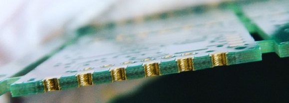
Plated half-holes allow for high-density, miniaturized electronic connections with ease of soldering and efficient board integration—two of the basic needs of modern PCB designs and applications today, such as WiFi modules.
The quickening pace of upgrading electronic products has given way to high-density, multifunctional, and miniaturized trends, thus the number of components on a PCB will increase squared, while that of the PCBs themselves will be radically decreasing. As a result, it will be necessary to have supporting boards. Round holes may introduce cold soldering when soldering a sub-board to a motherboard due to the volume of the round hole, hence leading to poor electrical connections. Plated half-holes were created as a remedy to this problem.
Definition
The copper plating, usually referred to as castellated half holes, on the edge of the PCB is within them, which is provided by a specialized process. These holes are used for board-on-board connections to enable the integration of different technologies. For instance, it can be combining complex microcontroller modules with more standard and individually designed PCBs.
One common application is the plugging of PCB modules like Bluetooth or Wi-Fi into another circuit board using plated half holes as the optimum technique. These holes result in SMD connecting pads. Because the PCBs are directly connected, the system's profile is significantly thinner than when multi-pin connectors are used.
Designs
The following points must be considered when creating plated half-holes.
- Placement: The centroid of any plated half-hole must be precisely on the PCB's edge or outline. When using elliptical holes, be careful with the start and finish positions.
- Definition: In your EDA software, define the holes/slots as PTH.
- File Requirements: When submitting Gerber files, remember to include the holes/slots in the drill file. For example: *.drills_pth.xln or *pth. DRL.
- Pad Stability: Each plated half-hole shall be contained within a pad on every copper layer. This shall be to provide stability to the copper sleeve.
- Pad Surrounding: Make sure that the pad covers the hole completely. The requirements for the pads and annular rings are the same as those for regular through-holes.
Minimum half-hole diameter: 0.6mm, but PCBX can go as small as 0.4mm. The edge-to-edge spacing between holes must be at a minimum of 0.55mm. If the distance falls between 0.47 and 0.55, expect an added cost and lead time. The smallest solder mask bridge is 0.1 millimeters.
Following these tips will allow you properly implement plated half-holes in your PCB design. Make sure to use the right parameters and dimensions in design and communicate promptly with your PCB manufacturer for production and assembly.
Manufacturing Process
The conventional process of manufacturing plated half-holes involves the following steps:
- Drilling
- Chemical copperization of the panel
- Image transfer
- Pattern plating
- Film stripping
- Etching
- Solder mask layer printing
- Surface treatment
- Hole formation
- Milling contours
These processes increase output and lower the performance of the product. However, such is not the case with modern processes. Plated half-holes require edge drilling of the substrate at their production, requiring specific equipment to avoid defects that will affect the subsequent process. Copper plating the holes after pretreatment enables components put on the circuit board to have strong conductivity.
Advantages
Easy handling and soldering: Because the holes are on the edge of the module, they are easier to solder, not so elusive as pads under the module that happen to make component installation complicated.
Easy measurement: Half-hole plating allows measuring distances between the hole and the solder more easily. Calipers can also be used after placing a module.
Coaxiality: Side-positioned holes have much fewer alignment errors compared to those under the module.
Cleaner Board Surface: Directly mounting a PCB module with plated half-holes to another board ensures less dust and dirt accumulation on the board surface.
Applications
- As branch boards for particular sections of large PCBs.
- Modifying the pin layout of components as per requirements by the user.
- As an integrated module connected on a single PCB, forming modules used during assembly.
- Easy direct assembly of a PCB with half-holes onto another PCB.
- Testing the quality of solder joints by interconnecting two boards.
- Applied in small modules like WiFi modules.
- Enabling wireless connections between PCBs and PCs.
Hot Tags:

Contact us

If you can't find what you're looking for, please contact us.
Article

Dive into our PCB glossary to master the key terms and definitions essential for efficient design and production, ensuring your projects run smoothly and effectively.
 2024/08/06
The trend towards lead-free PCB manufacturing comes due to the EU's ROHS directive, which requires compliance to the limits on the content of lead. Compliance with lead-free is achieved by different surface finishes such as ENIG, ImAg, ImSn, and OSP—all with their different pros and cons. This paper compares these finishes to help choose the best for specific PCB applications.
2024/07/29
One is a bare circuitry board, and another has all the components and is functional: PCB stands for Printed Circuit Board, and PCBA stands for Printed Circuit Board Assembly. PCB acts like a base, and components are assembled on it at a later stage through various methods in PCBA, such as SMT and Thru-Hole Technology.
2024/07/29