What is Solder Mask?
Solder mask, or solder resist, is the polymer layer on PCBs that protects against oxidation, short circuits, and solder bridges. Types include LPI, dry film, and epoxy, chosen based on design, application, and cost.
A Solder Mask, also known as Solder Resist, consists of a layer of polymer material applied on the surface of a Printed Circuit Board-PCB. This coating is applied to protect a PCB against potential oxidation apart from avoiding any accidental solder bridges between adjacent traces while performing the soldering process. Solder mask usually comes after the copper traces and vias have been etched and solder pads have been plated. Materials commonly used for solder mask include thermoset epoxy and liquid photoimageable (LPI) solder mask. It is applied in such a pattern that the copper pads and vias, which are to be soldered, expose, while the rest of the places-which are not to be soldered-are called "lands".
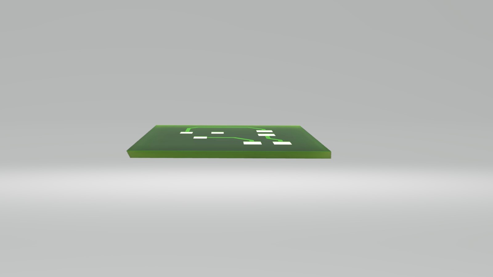
Purposes of Solder Mask
Solder masks are applied on top of the solder side of a PCB. Their major functions include:
Protection: The mask covers the copper traces from oxidation and corrosion due to environmental factors, hence enhancing the durability and reliability of a PCB.
Insulation: The solder mask insulates the adjacent copper traces from each other, hence preventing the possibilities of short circuits from mislaid solder or other kinds of contamination.
Solder Bridging Prevention: It avoids the possibility of solder sticking to wrong places of the PCB, hence avoiding solder bridges that would present electrical faults.
Aesthetic Appeal: The solder mask helps the PCB present a uniform, professional appearance, making some aspects of visual inspection easier. Various colors can also be applied for branding purposes or differentiating between different types of PCB.
Common Types of Solder Masks
Below is an overview of the three most common types of solder mask and their respective advantages and disadvantages:
Liquid Photoimageable, or LPI, Solder Mask
LPI is the most commonly used type of solder mask. Applied as a liquid, LPI is exposed to ultraviolet light for hardening.
Pros: High resolution; hence, suitable for fine features and high-density PCBs. Color: Available in wide range.
Cons: More expensive than other types and UV light is required for its cure.
Dry Film Solder Mask
Dry film solder masks are processed by applying pre-made film onto the PCB, followed by lamination and curing. Normally used in high temperatures for automotive or aerospace electronics-based applications.
Pros: Provide good chemical and mechanical resistance; best suited for use in high-temperature applications.
Cons: Limited colour options; not suitable for fine features.
Epoxy Liquid Solder Mask
Epoxy solder masks are applied as a liquid and then cured with heat. They can be found in applications that require a great deal of durability, such as industrial control systems and medical equipment.
Pros: It provides very good adhesion, with excellent mechanical strength; thus, suitable for durable applications.
Cons: Colour limitation and perhaps more difficult to apply compared with other types.
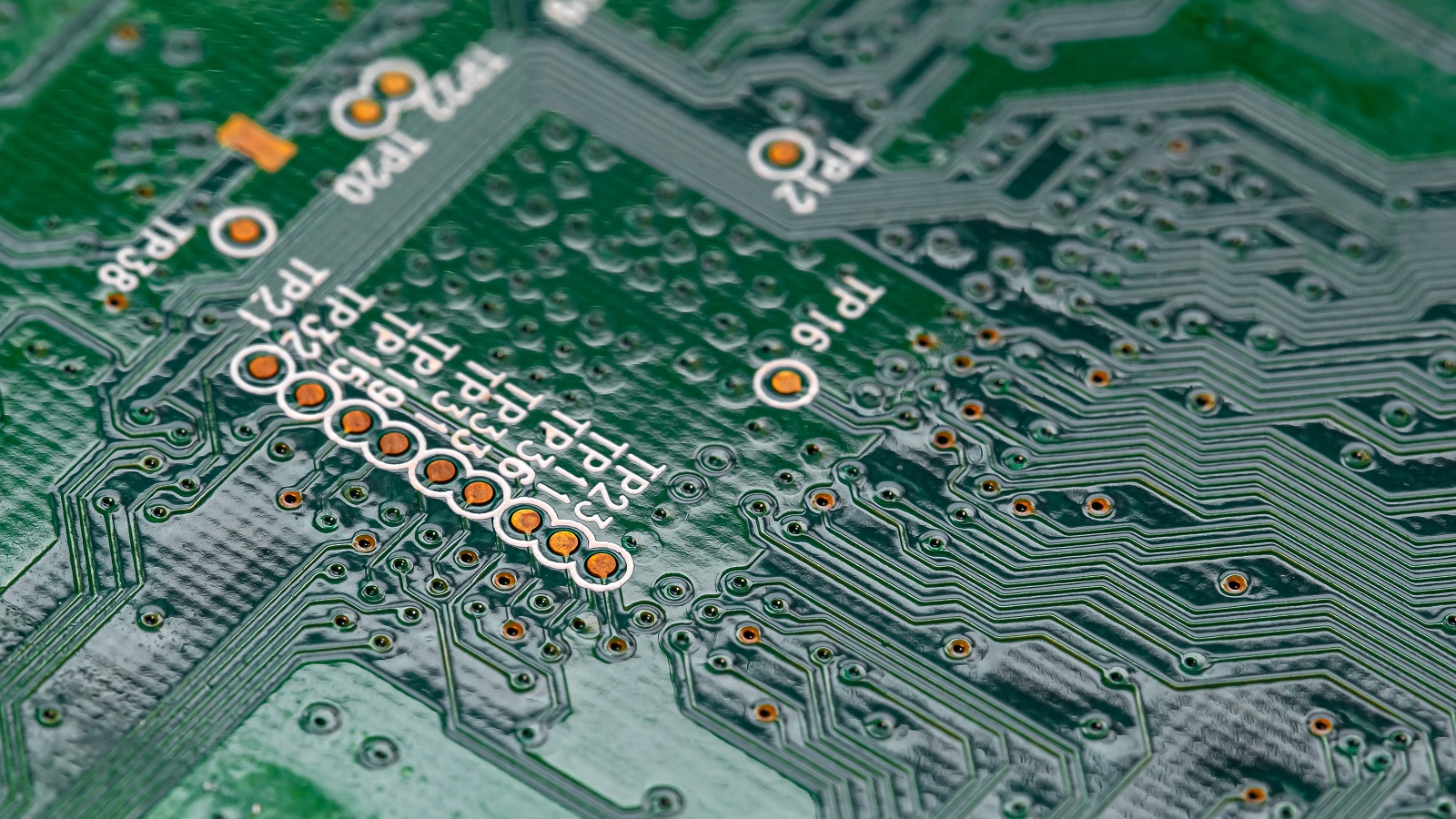
Selection Factors for Solder Mask
In choosing solder mask for a given PCB, a number of factors need to be put into consideration and these include:
PCB Design: High-density PCBs would require solder masks with high accuracy and resolution such as LPI.
Application: The PCB application will drive the selection of solder mask because it could be in mechanical or even at high temperatures.
Cost: It can be determined by budget in some cases because not all solder masks are equally expensive.
Color: Tend to vary depending on the differentiation of PCB components or depending on aesthetic requirements.
How to Apply Solder Mask on a Printed Circuit Board
The application of solder mask would normally involve several steps for it to be able to work effectively:
Cleaning and Preparation: Thorough cleaning is carried out on a PCB to ensure that there is no kind of contamination that can prevent solder mask adhesion.
Solder Mask Application: Some of the common techniques used in this process are screen printing, spray coating, or inkjet printing, but by far, the most used technique is screen printing.
Solder Mask Curing: Allow applied solder mask to cure under either heat or UV light; it hardens and provides good adhesion.
Inspection of PCBs: Inspect the PCBs for defects such as incomplete coverage. Any noted issues will need repair before further processing of the PCB.
Proper application and curing of the solder mask is thus essential to a reliable operating PCB.
Conclusion
Solder masks play a major role in the manufacture of PCBs for protection, insulation, and aesthetic reasons. The type of solder mask that will be used would depend on the design of the printed circuit board, its operating environment, and the budget allocated for that particular product. Being able to understand the types and their respective advantages is helpful in making informed decisions about the reliability and performance of the final product. A solder mask applied and cured well really enhances quality and durability in PCBs, which become important in different high-demanding industries.
Hot Tags:
Contact us

If you can't find what you're looking for, please contact us.
Article
The article provides a step-by-step guide to soldering a PCB, covering workspace setup, essential tools, and safety measures. It explains heating the soldering iron, applying flux, tinning the iron tip, placing components, heating joints, applying solder, cooling, inspecting, and cleaning. Emphasis is on practice and safety for successful soldering.
PCB conformal coating is a thin, non-conductive film applied to circuit boards to protect them from moisture, dust, and temperature variations. Made from materials like acrylics and silicones, it provides insulation and corrosion resistance. Application methods include brushing, spraying, dipping, and vapor deposition.
Wave soldering is a PCB assembly process that moves the board over a molten solder wave to create reliable connections. Evolving from dip and drag soldering, it offers consistent, high-quality solder joints. Despite its complexities, it remains essential for through-hole components and complex PCB assemblies.