- Products & Capabilities

- About
- Resources
What is a PCB Hole and Via Difference?


PCBs are central to electronic devices, featuring holes and vias critical for functionality. Holes, like through-holes and mounting holes, serve electrical or mechanical purposes, while vias ensure electrical connections across PCB layers. Understanding their differences is key for optimal performance, reliability, and manufacturability in PCB design.
In this dynamic world of electronics, everything electronic has in its heart a printed circuit board. From your smartphones, computers, and industrial machinery down to some of your modern household appliances, PCBs form the backbone in today's gadgets. In designing and manufacturing PCBs, one needs to know and understand several types of holes and vias that are common features of every PCB. While the terms "holes" and "vias" may sound somewhat synonymous, they do hold different purposes and specific characteristics critical to the performance and functionality of a PCB. This article will elaborate on the differences between PCB holes and vias with in-depth information about their function, types, construction, and usage in PCB design.
PCB Holes
A "PCB hole" generically refers to any opening drilled into the PCB substrate. Holes in PCBs may serve either electrical or mechanical purposes. Holes represent an integral part of the structure and functionality of a board, accommodating components and hardware.
Types of PCB Holes
1. Through-Hole
Description: Thru-holes are completely drilled openings running from one side of the PCB to the other. These usually serve for Thru-hole technology components-resistors, capacitors, and integrated circuits with wire leads through the PCB-soldered on the opposite side.
Purpose:
Component Mounting: Essentially, the thru-holes are used for mounting and fastening electronic components with extended leads through the PCB.
Electrical Connectivity: Although basically mechanical, through-holes provide electrical connectivity when the component leads are soldered to the copper pads on the PCB.
2. Mounting Hole
Description: Mounting holes are normally non-plated holes used for mechanical purposes. They allow no electrical connections but are very important in holding the PCB within its enclosure or mounting it onto some other structure.
Purpose:
Mechanical Attachment: It is used to screw down screws, stand-offs, or other hardware meant for mechanical attachment in place.
Isolation: It sometimes provides isolation between different sections in a multi-board assembly.
Construction and Considerations
Drilling Process: The application of holes in a PCB involves a precision drilling process where the PCB undergoes drilling before additional manufacturing steps for it may be performed, such as layering and plating.
Plating: Based on requirement, some holes would be plated with copper for good solder adhesion and mechanical stability, and others without plating.
Design Considerations: Addition of holes impacts on routing and space in a PCB. A designer has to very carefully place the holes so as not to interfere with signal paths and other components.
Vias
A via is another special kind of hole that is designed specifically for electrical connections between different layers of a multilayer printed circuit board. Unlike regular holes, vias are always made with a copper plating to ensure the best electrical paths.
Types of Vias
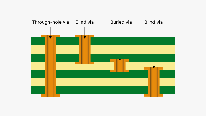
1. Through-Hole Via
These vias are the ones that go through the whole PCB from top layer to bottom. They connect all the layers they go through.
Purpose:
Layer-to-Layer Connectivity: It provides electrical connectivity between disparate layers in a multi-layer Printed Circuit Board that enables complex circuitries.
Usage: They are used very frequently in tracking signals, power, and grounds across layers.
2. Blind Via
Blind vias connect an outer layer with one or more inner layers without reaching all the way through the PCB.
Purpose:
Space Efficiency: Since the via is required to occupy only those layers which are really necessary, it saves more surface area of the PCB for component placement and routing.
Reduced Complexity: Due to the via depth limitation, it reduces the complexity in managing signal integrity by reducing stray capacitance.
3. Buried Via
There are some vias that connect only the internal layers of the PCB without going to the outer layers.
Purpose:
Complex Routing: It allows for complex internal layer routing without hampering surface layers for high-density and complex PCB design.
Signal Integrity: The signal and power integrity is maintained by managing the internal layer connections through them effectively.
Construction and Considerations
The vias are first drilled and then copper-plated for good electrical conductivity. For microvias, HDI PCBs use advanced manufacturing techniques such as laser drilling.
Parasitics and Signal Integrity: Vias add some parasitic inductance and capacitance to the overall circuitry. These may weaken the performance of high-speed signals. Such issues must be taken into consideration during the design process for very high-frequency and high-speed PCB designs.
Design Implications: There are strong influences on the performance of a PCB based on via placement and type. Adequate via management should be carried out to ensure that no problems in signal integrity, thermal issues, or added manufacturing costs arise.
Comparing PCB Holes and Vias
Functional Differences
Mechanical vs. Electrical:
PCB Holes: Those are mainly for mechanical mounting when they constitute mounting holes and electrical/machine when they are for through-hole components.
Vias: Vias are used strictly for electrical connectivity between the different layers of the Printed Circuit Board.
Design and Layout:
PCB Holes: Placement is to a great extent decided by component and assembly requirements.
Vias: Placement is one of the prime considerations in the electrical design. It will affect not only signal routing but also impedance control and even thermal management.
Construction and Manufacturing
Drilling Techniques:
PCB Holes: Generally drilled using mechanical drills. The processing technique is simpler but needs precision to achieve the proper positioning.
Vias: Often utilize advanced techniques such as laser drilling, especially when microvias are used in HDI boards.
Plating:
PCB Holes: Either plated or unplated depending on the function.
Vias: Always plated for the electrical connectivity across layers.
Design Implications
Routing and Space Utilization:
PCB Holes: Affect the available space for routing other traces or placing more components.
Vias: Affect the routing strategy and stack-up design. Efficient via management has the potential to make profound improvements in the performance of the PCB.
Thermal Management:
PCB Holes: Through-plated holes can aid in thermal management by allowing heat to dissipate through the board.
Vias: Thermal vias are designed to channel heat away from critical components toward heat sinks or dissipation areas.
Conclusion
First of all, to effectively and reliably design printed circuit boards, one should understand the difference between PCB holes and vias. Though both are integral components with respect to the functionality of the PCB, they serve different purposes: whereas PCB holes are important with regard to mechanical stability and component placement, vias are about providing critical electrical pathways between layers. An effective PCB design exploits these two in the best way to yield the optimal performance, reliability, and manufacturability of the board.
Whether you're an experienced PCB designer or you're just entering this area, being able to appreciate the nuisances of holes and vias will surely enhance your design capability and result in better electronic products. In the competitive world of electronics, the devil is always in the details, as knowing these sometimes minor differences makes all the difference in the success of your projects.
Hot Tags:

Contact us

If you can't find what you're looking for, please contact us.
Article
Vias—blind, buried, and through-hole—are essential in multi-layer PCBs, enabling signal and power transfer between layers. Covering techniques like tenting and plugging with solder masks enhance PCB reliability and performance, crucial for compact designs.
 2024/09/11
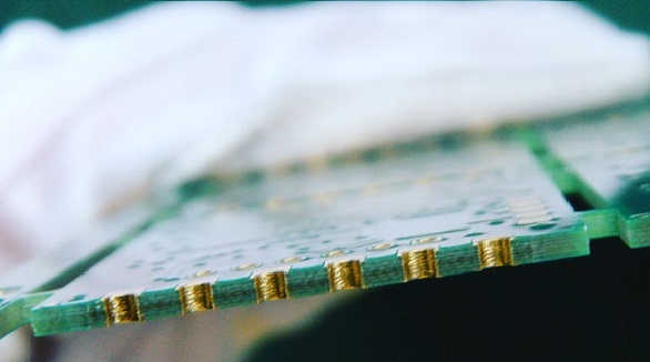
Plated half-holes allow for high-density, miniaturized electronic connections with ease of soldering and efficient board integration—two of the basic needs of modern PCB designs and applications today, such as WiFi modules.
2024/07/29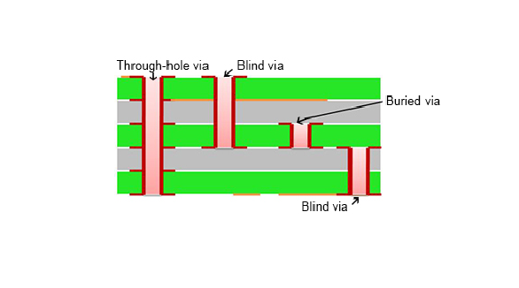
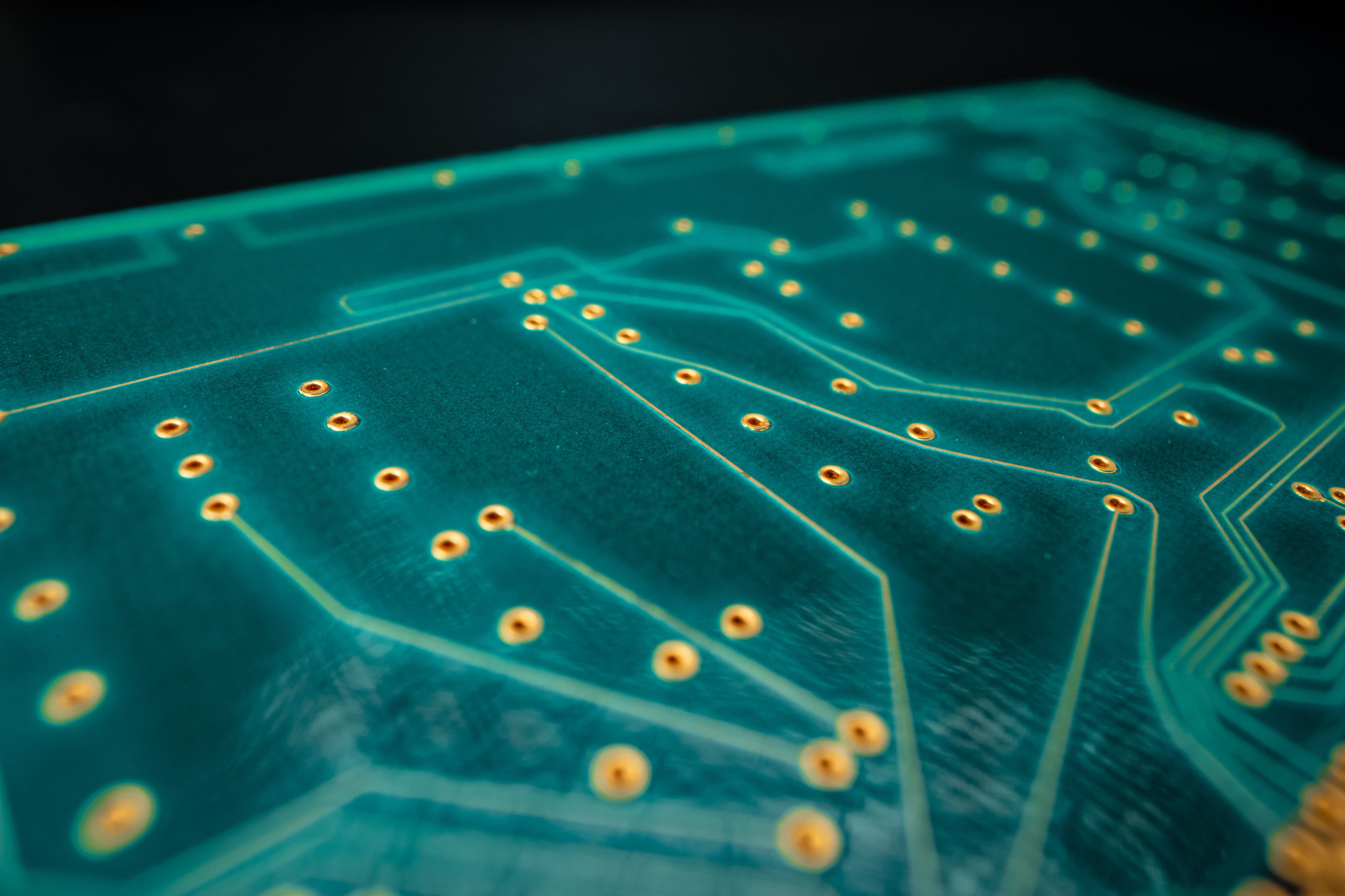
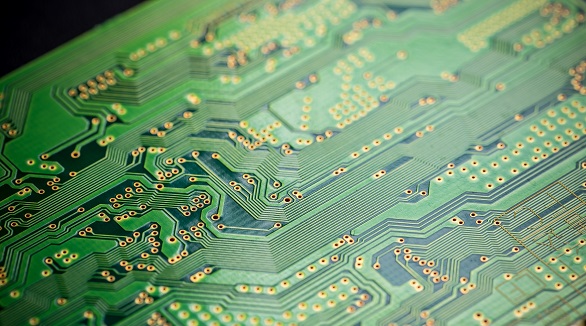
A printed circuit board includes a number of copper foil circuits, which are interlinked by vias. Via (through-hole, blind, buried, stacked, microvias) provides critical interlayer connections in high-density interconnection boards. Blind and buried vias increase the density of boards without adding size; hence, they are imperative for modern trends of miniaturization and high-speed signal transmission. These vias are plated with conductive materials, usually copper, so the electron flow can happen without much effort. Although advanced via types, like stacked vias, cost more, they save up much space and significantly improve routing capacity.
2024/07/26