- Products & Capabilities

- About
- Resources
What is a Via in PCB?


Vias—blind, buried, and through-hole—are essential in multi-layer PCBs, enabling signal and power transfer between layers. Covering techniques like tenting and plugging with solder masks enhance PCB reliability and performance, crucial for compact designs.
The term "via" is very wide and is an integral part of electrical engineering in the design process of multi-layer Printed Circuit Boards or simply, PCB. From the Latin word for "way", the "via" makes a very critical contribution to the functionality of PCBs, allowing for the transfer of electrical signals across different layers. Notably, the concept of a via can be obscure to many. This article will try to rid this ambiguity by exploring what a PCB via is, how it works, its types, and the processes involved in covering it.
What is a Via?
The simplest form of a via is just a small, drilled hole passing through two or more adjacent layers of a multi-layer PCB. These drilled holes allow the passage of electrical signals and power between the layers, thus making it possible that complex pathways within a circuit are possible. Since various layers of a multi-layer PCB are relatively independent, vias play a significant role in interlayer interconnects.
Vias can be broadly categorized into three types based on their functionality—blind via, buried via, and through-hole via.
Functions of Via
The major purpose of vias within a PCB is to create an electrical path between the different layers on the board. Normally, there are several layers in a PCB so that such an intense network of traces and components can be accommodated. Vias allow the flow of electrical signals and power between layers; this is a way of making different components and portions of the circuit interconnected in an efficient manner.
Here is how some of the important roles of vias are played in PCBs:
Inter-Layer Connectivity: The via, on its part, allows signals and power to travel to other layers in the PCB.
Inter-Layer Connections: Vias enable the conduction of signals and power to other layers of the PCB, connecting traces and components on one layer to another. It becomes critical for multilayer PCBs when, most of the time, there is no space left or it's impossible to route on surface layers only.
Component Interconnection: Vias are important for interconnecting components across different layers of PCBs. This is especially required when compact, closely packed circuits require the space in which to mount components to be very close.
Efficiency in Routing Signals: Via allows the routing efficiency. If there would have been no vias, the traces would have had to snake through the surface layers, wasting even more space, and probably interfering with signals. Vias allow routing signals through a PCB much more directly and with good space saved.
It plays an important role in **Power Distribution**: Vias may also be used in the interconnection of different-layer powers to planes that distribute power to various components along the board.
Minimizing Signal Distortion: In high frequency and high-speed applications, beyond doubt the vias will affect the signal integrity; therefore, good design and placement of vias can minimize signal distortion. Reflections and impedance mismatch problems that will raise the performance of the PCB.
Utilization of Space: Vias make space utilization possible on a PCB because they can be used in multi-layer designs and would eventually prove to be good for routing activities, ensuring that the conduction would be done right. This applies to modern small and compact electronic gadgets.
High-Density Interconnect: Microvias are parts of advanced PCB designs for fine pitch designs that ensure the gadgets get miniaturized further with the use of HDI technology.
In this regard, vias form the most vital components in PCB design, acting as the carrier for electrical linkage among its layers, thus contributing to efficiency, reliability, and compactness of electronic circuits. Design and placement of these elements are thus very critical in various applications.
Types of Vias
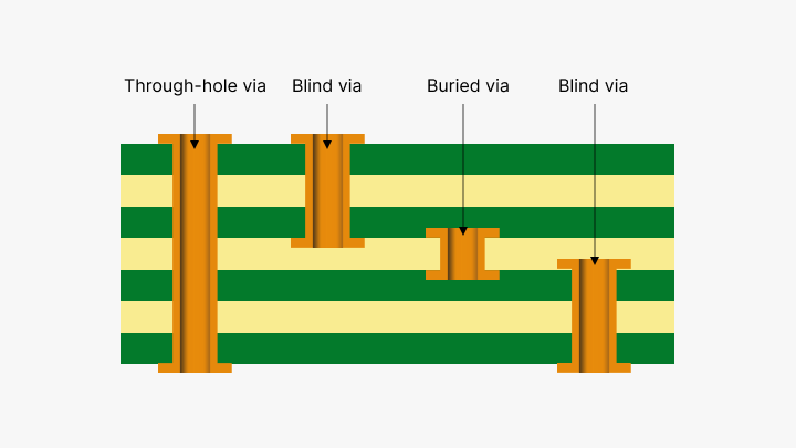
Blind Via
The blind via is a small hole that starts from one surface of the PCB, but doesn't pass all the way through to the other side. One of the main advantages of blind vias is that they occupy no real estate on all the layers. It gives extra room to increase design density, particularly in small designs. And for that matter, they are often applied in high-bundle-density circuit packs like ball grid arrays and high-density interconnect PCBs.
Buried Via
Buried vias are connections involving at least two inner layers but not reaching the outer layers, and hence they can't be seen from the outside. It is this aspect of invisibility that makes them quite effective in reducing electromagnetic interference between the signals, thus improving the reliability and performance of the PCB as a whole. Buried vias are quite important in HDI PCBs, where space is at a premium and signal integrity needs to be maintained.
Through-Hole Via
The most common variant used in the manufacture of PCBs is the through-hole via. It is a hole passing throughout the PCB, somehow interconnecting the inner and the outer layers in a very straightforward way. Through-hole vias mostly find applications in internal board interconnections; however, they can act as mounting holes for different components. Because they are rather simple to be manufactured, through-hole vias find broad application in a surprisingly large range of designs for PCBs.
Covering Vias
PCB vias can be covered or finished using three methods: tenting of vias, vias not covered, and plugged vias with solder mask.
Tenting Vias
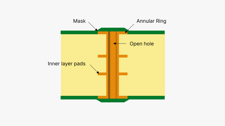
Tenting vias involves covering the annular ring, the visible part of the ring surrounding the via hole, with a solder mask for insulation. This solder mask forms a protective layer to prevent any type of accidental electrical connections. For insulation to be proper, the annular ring must be entirely covered with a thick enough solder mask to prevent the chances of an accidental short circuit.
Vias Not Covered
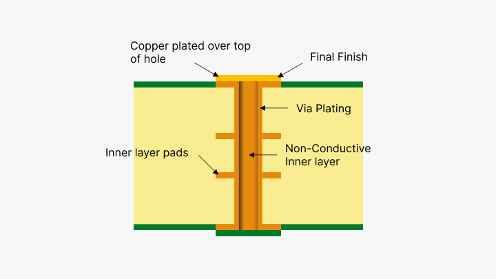
If the vias are left uncovered, it mostly leads to the hole and the annular ring being exposed. This may actually be of potential benefit in debugging, as access to measurement signals is easier with an exposed probe point. More importantly, it helps in heat radiation from the board by increasing the exposed surface area. The downside is increased risk of short circuits due to exposed conductive parts.
Plugged vias with solder mask fill the via holes with some kind of solder mask, which in turn closes the via. This will avoid the generation of solder balls in the wave soldering process and avoid flux residue inside the via hole. Therefore, this method is often used to design PCBs that incorporate BGA or IC assemblies. This process seals the vias to ensure far more safety and efficiency during the manufacturing and operational phase.
How to Select the Right Via?
The choice of via type depends on the needs of the PCB design. Blind and buried vias offer space-saving and a higher signal integrity, but they are only possible on boards containing four or more layers, and they are considerably more complicated and expensive to produce. On the other hand, through-hole vias are simpler and less costly, so they normally find preference in standard designs for PCBs.
Conclusion
Knowing what a Via is and how it works is the bottom line of PCB design and manufacturing. Vias—blind, buried, and through-hole—are the critical paths used to connect complex multi-layered boards. The vias are covered with different methods: tented, with photoimageable solder mask, or plugging. These differ in meeting the various needs to raise the efficiency, reliability, and functionality of today's PCBs.
The nuance of via design and application becomes ever critical to both engineers and manufacturers as compact and high-performance printed circuit boards continue to rise in demand. If the designers choose the right vias and covering methods, they shall be able to compose advanced, reliable, and highly functional PCBs.
Hot Tags:

Contact us

If you can't find what you're looking for, please contact us.
Article
PCBs (Printed Circuit Boards) are fundamental in electronics, composed of multiple layers like silkscreen, soldermask, copper, and substrate, chosen for specific electrical functions.
 2024/08/07
The trend towards lead-free PCB manufacturing comes due to the EU's ROHS directive, which requires compliance to the limits on the content of lead. Compliance with lead-free is achieved by different surface finishes such as ENIG, ImAg, ImSn, and OSP—all with their different pros and cons. This paper compares these finishes to help choose the best for specific PCB applications.
2024/07/29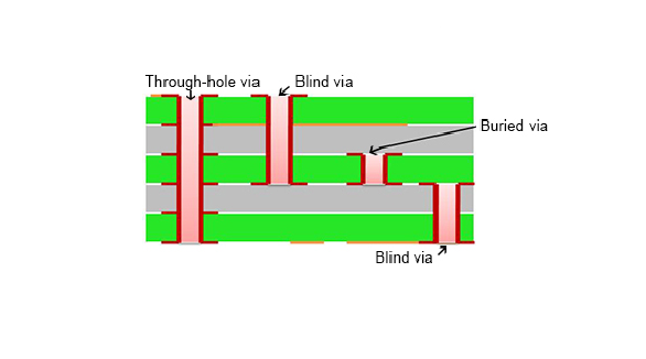
A printed circuit board includes a number of copper foil circuits, which are interlinked by vias. Via (through-hole, blind, buried, stacked, microvias) provides critical interlayer connections in high-density interconnection boards. Blind and buried vias increase the density of boards without adding size; hence, they are imperative for modern trends of miniaturization and high-speed signal transmission. These vias are plated with conductive materials, usually copper, so the electron flow can happen without much effort. Although advanced via types, like stacked vias, cost more, they save up much space and significantly improve routing capacity.
2024/07/26