- Products & Capabilities

- About
- Resources
What is the Difference Between Pad and Via in the PCB?


Pads and vias are crucial for PCB design: pads serve as soldering points for components, while vias connect different layers. Understanding and correctly implementing them ensures reliable, efficient, high-performance PCBs.
Printed Circuit Boards presently play an important role in modern electronics, enabling complicated circuits to become compact, reliable, and efficient. In the case of the Printed Circuit Boards, there are two critical elements: Pads and vias, which serve different unique and essential functions. Although they always come in a pair, they are for different functions concerning the board layout. Understanding these differences will be crucial to effective PCB design and manufacturing.
What is a Pad?
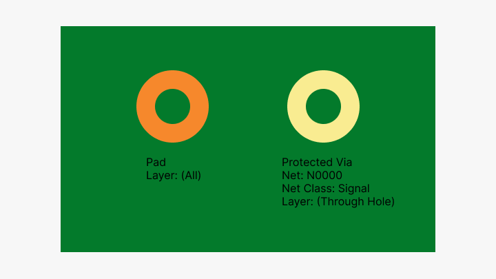
Pad or soldering pad is, on a PCB, an area to which the lead of a component or the terminal is to be soldered. These small exposed areas of metal form an integration point for components, land pattern - binding or positioning it, and electrical attachment to the board.
Types of Pads
Pin Pads: Pin pads are the kind of pads with soldering holes. They are basically utilized for through-hole components. Such components have their leads through the board to the opposite side, where they are soldered on.
Surface Mount Pads: Surface mount pads do not contain soldering holes. They are used for surface mount technology components, which are soldered directly onto the pad atop the board.
A Pad performs the function of mechanically and electrically securing components to the board with reliable connectivity in the circuit.
What is a Via?
A via, or vertical interconnect access, is a small hole drilled into the PCB for connecting traces between different layers. Vias are very important in multi-layer or double-sided boards to route signals or voltages vertically through the board in order to connect various layers.
Types of Vias
Plated Through-Hole (PTH) Vias:
These vias run from the top layer to the bottom layer and connect all the layers in between.
Blind Vias:
Blind vias are those extending from an outer layer either from the top or bottom to one or more inner layers without reaching the opposite side.
Buried Vias:
Buried vias come totally within the inner layers of a PCB and never reach either of the outer layers.
Microvias:
Very tiny vias, and usually laser-drilled. Microvias are a feature of High-Density Interconnect HDI PCBs.
The main function of vias, however, is to route signals across multiple layers of PCBs, hence enabling more complex and compact designs.
Key Differences Between Pads and Vias
Understanding the differences between a pad and a via is indispensable for any professional dealing with the design of printed circuit boards :
Function and Purpose:
Pads: Represent the main soldering points for components and provide the required mechanical and electrical connections on the surface of the board.
Vias: These provide electrical interconnection between different layers of the printed circuit board. They make multi-layer routing possible without using any surface area.
Structural Considerations:
Pads: They are meant to be mechanically strong enough to bear the severe stresses during the installation of the components and while soldering them, so that for this reason they have a sufficient diameter, to allow the lead of the component end.
Vias: Smaller apertures are needed, focusing on keeping electrically joined layers together. The smaller vias sometimes may be more expensive because of precision in drilling and plating processes.
Design Considerations:
Pads: There is a need to ensure spacing appropriately, pad diameters, and solder mask clearance for good soldering and reliable connections.
Vias: Consider thermal and electrical properties, minimize problems such as noise and reflection in signals. This is achieved by the optimal implementation of via size, its placement, and dimensions of the annular ring.
Detailed Insight into Pads
The size of the aperture in the Pad should be at least big enough to clear the component pin. Because the drilling process can be a bit sloppy, the aperture will, in general increase about 0.15 mm. So for example, with a designed hole diameter of 0.5mm, after drilling it could be around 0.65, so the final aperture would be approximately 0.55mm after copper immersion
Regarding the Pad structure, there should be at least 0.20 mm width in the soldering ring to ensure reliable adhesion and electrical connectivity.
Detailed Information on Vias
Vias are involved with a high level of drilling and plating art in manufacture. Within most Chinese PCB manufacturing enterprises, the general PTH diameter is about 8 mil (0.2 mm), while BVH has a diameter of 4 mil (0.1 mm). Because of the production process, the final actual aperture of a via will be about 0.1 mm less than the size planned for it. That is to say, after the copper immersion process, a via designed to be 0.5 mm in diameter may have an actual diameter of about 0.4 mm. Usually, in order to ensure good electric connections, the soldering ring of the via should be at least 0.15 mm wide.
Via-in-Pad
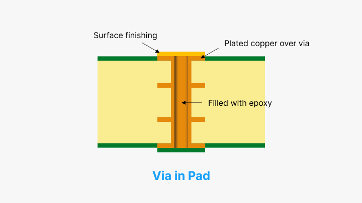
In high-density PCB design, space optimization is critical, and creative routing solutions often used include via-in-pad. In via-in-pad design, vias are placed underneath the surface mount component pad. This helps to provide space on the surface for other components and can help towards better routing efficiency, thermal dissipation, and inductance reduction.
However, via-in-pad designs are more challenging and more expensive. Via size is also a critical issue because larger vias can have unnecessarily high resistance. Vias need to be placed correctly to reduce noise without impacting signal integrity; annular rings should also be suitable to maintain electrical and thermal integrity. Moreover, the solder mask design too needs to be such that it prevents solder from wicking into the via itself during the assembly.
Conclusion
Understanding the difference between pads and vias is very important for effective PCB design. While pads are responsible for component placement and electrical connections along the board surface, vias provide interlayer connections, very important in multi-layer PCB designs.
While both pads and vias are used for different purposes, appropriate design and implementation of the same are quite important for the development of reliable and high-performance PCBs. From simple single-layer boards to complex multilayer designs, recognizing and appropriately using the respective functions of pads and vias will do much good in efficiency and functionality for your electronic project.
By mastering these aspects, PCB designers can make well-informed choices that optimize both the design and manufacturability of their boards, ensuring robust performance and cost-effective production.
Hot Tags:

Contact us

If you can't find what you're looking for, please contact us.
Article
PCBs are central to electronic devices, featuring holes and vias critical for functionality. Holes, like through-holes and mounting holes, serve electrical or mechanical purposes, while vias ensure electrical connections across PCB layers. Understanding their differences is key for optimal performance, reliability, and manufacturability in PCB design.
 2024/09/11
Vias—blind, buried, and through-hole—are essential in multi-layer PCBs, enabling signal and power transfer between layers. Covering techniques like tenting and plugging with solder masks enhance PCB reliability and performance, crucial for compact designs.
2024/09/11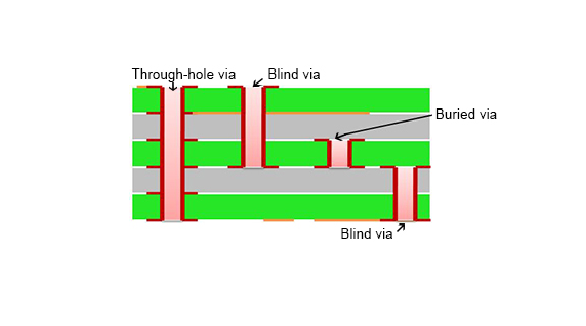
A printed circuit board includes a number of copper foil circuits, which are interlinked by vias. Via (through-hole, blind, buried, stacked, microvias) provides critical interlayer connections in high-density interconnection boards. Blind and buried vias increase the density of boards without adding size; hence, they are imperative for modern trends of miniaturization and high-speed signal transmission. These vias are plated with conductive materials, usually copper, so the electron flow can happen without much effort. Although advanced via types, like stacked vias, cost more, they save up much space and significantly improve routing capacity.
2024/07/26