What is the Photoresist in PCB Board?
Photoresists are crucial in PCB fabrication, with negative types offering cost efficiency and positive types providing high resolution for detailed designs.
In the highly complicated process involved in making printed circuit boards, photoresist materials provide the essential function that allows photolithography to facilitate such precision in modern electronic devices of today. Knowing the differences and applications of negative and positive photoresists is quite indispensable in any high-quality production of PCBs. The article describes the application of and differences between these two types of photoresists, underlining their importance in the process of fabricating a PCB.
Photolithography is the basic method in the production of a printed circuit board. Primarily, this process depends on photoresist materials sensitive to light for the transferring of intricate circuit patterns onto a substrate. The process is important in developing tiny and accurate designs applied in many electronic applications. The process involves two basic stages: development of "artwork" describing the design of the circuit, and the "masking" process, in which this design is transferred onto a PCB through the action of photoresist.
Negative Photoresist vs. Positive Photoresist
There exist two major types of photoresists in photolithography, the negative and positive photoresists, which have different properties as well as applications:

Negative Photoresist
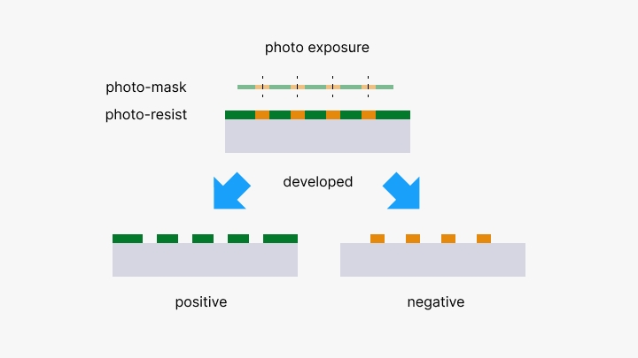
The negative photoresist becomes rigid upon exposure to UV radiation. In such a process, a negative version of the circuit pattern is applied hence; areas that are exposed will be kept after development while areas not exposed are washed away.
Applications: Negative photoresist is applied in cases where cost efficiency is the key factor. These photoresists are mainly applied in situations that do not require ultra-high resolutions.
Advantages: It is cheaper compared to other positive photoresists.
Less complicated in design and can, therefore, be used where extreme precision is not needed.
Disadvantages: Has a lower resolution; about ¼ of what is achievable with positive photoresists, thereby limiting its application to very detailed circuit designs.
Positive Photoresist
The positive photoresist, on the other hand, after exposure in UV radiation, becomes soluble and therefore is removed during the development process. A positive image of the circuit applied provides a far greater degree of accuracy in the final PCB.
Application: More precisely for high-resolution and fine designs, the use of positive photoresist would be apt for thickly set circuit layouts in modern-day electronics.
Advantages: Provides roughly four times the resolution of negative photoresist, hence ideal for complicated designs, which is better suited for advanced PCB applications where space is limited and precision is required.
Disadvantages: Generally more expensive with consequently higher production costs.
The Role of Photoresist in PCB Manufacturing
Artwork and Photomask Preparation
Photolithography involves the creation of "artwork" for the circuit. Designs of artwork can be pre-made in minute detail using CAD programs. Designs are used to develop photomasks depending on whether the process to be applied is a positive or negative photoresist.
Positive photomasks are generated for application in positive photoresists where there is a need for higher precision.
Negative photomasks relate to negative photoresist processes, which one can adopt for simpler designs.

Photoresist Coating and Development
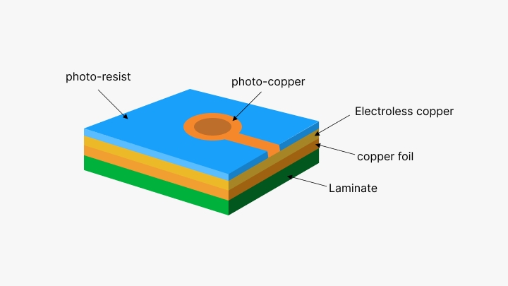
Application: The photoresist may be applied as either a liquid or as a dry film onto the board. Dry films usually yield more consistent coverage and are much easier to handle in controlled environments. To expedite product processes for manufacturers, pre-sensitized PCB blanks coated with either positive or negative photoresist are available.
Exposure: The coated PCB is masked with artwork and then exposed to UV light. Whether the exposed or the unexposed area that stays behind will be determined by the type of photoresist used.
Development: The board is then treated with a developer solution after being exposed. In the case of positive photoresist, the exposed areas dissolve, leaving behind a precise pattern of the desired circuitry. In negative photoresist, the unexposed areas are removed; hence, the design that has been structured by the photomask remains.
Choosing Between Positive and Negative Photoresist
Many factors come into play while one decides between positive and negative photoresist:
Resolution Requirements: For designs requiring very high resolution, positive photoresist is more useful due to its higher resolution capability.
Cost Issues: Projects in which cost could be an major issue, and very high resolution is not called for, might use negative photoresist.
Manufacturing Flexibility: In general, for projects with complicated design considerations, the use of positive photoresist is superior due to its resolution and flexibility factors.
Photoresist materials are an indispensable part of the manufacture of PCBs, and it is this step that ensures quality and functionality of the pattern. Being able to understand the difference between photoresist negatives and positives, and in what contexts they can be used, will provide the ability for manufacturers, like PCBX, to optimize production to provide excellence in functionality and aesthetics for electronic components. The application of either positive or negative photoresist in the fabrication of PCBs, if done with complete insight, improves performance and reliability, further allowing efficient space management and precision in advanced electronic solutions. Mastery of these techniques enables PCB manufacturers to meet the demand for quality and durability that has recently characterized the rapidly evolving market for electronic devices.
Hot Tags:
Contact us

If you can't find what you're looking for, please contact us.
Article

PCB panelization consolidates multiple PCBs into a larger board, improving manufacturing efficiency and reducing waste. Techniques include V-scoring and tab-routing. Proper design enhances assembly, testing, and cost-effectiveness.

PCBs are essential for electronic devices, providing mechanical support and electrical connections. This article explores the importance of PCB panel dimensions, standard sizes, and optimization techniques. Key points include cost-efficiency, ease of manufacturing, quality control, and optimal layouts. Factors like board size, volume needs, and equipment capabilities influence panel size. Coordination with manufacturers, using design software, and employing standard sizes can enhance production efficiency and quality.

Backplane PCBs support functional boards, distribute power, and transmit signals. Increased IC complexity demands more layers and high performance, creating challenges in alignment, drilling, electroplating, ICD issues, and stub management. Tips include precise alignment control, advanced drilling and plating techniques, and maintaining stub lengths below 0.25mm for optimal signal quality.