- Products & Capabilities

- About
- Resources
Which Surface Finish is Right for Your PCBs?


The trend towards lead-free PCB manufacturing comes due to the EU's ROHS directive, which requires compliance to the limits on the content of lead. Compliance with lead-free is achieved by different surface finishes such as ENIG, ImAg, ImSn, and OSP—all with their different pros and cons. This paper compares these finishes to help choose the best for specific PCB applications.
The trend towards lead-free PCB (Printed Circuit Board) came from the European Union directive called ROHS: the Restriction of Hazardous Substances, stating that any electronics would have to be obeyed by the ROHS direction placed upon them. This, in turn, led to the transition from lead-based processes to lead-free manufacturing of PCB.
Plated pins of components, PCB plated pads, and solder are important sources of lead in solder joints. To ensure that the lead content of the solder joint complies with ROHS regulations which request that mass fraction is less than 0.1%, the surface finishes for use in PCBs have to satisfy lead-free requirements. Many surface finishes have been developed to support lead-free fabrication, and the most popular of which are ENIG, ImAg, ImSn, and OSP.
Since each type of surface finish has different advantages and disadvantages, it is quintessential that you choose which one will best work for your projects. This article compares the four surface finishes based on application conditions, cost, lead-free compatibility, shelf life, solderability, etc to help pick out the best surface finish for your lead-free PCBs.
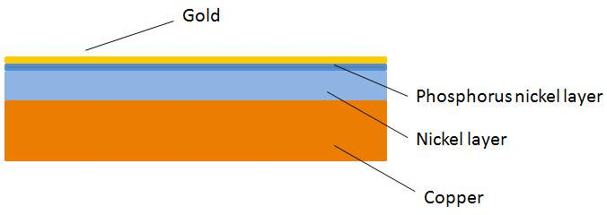
ENIG
ENIG is the abbreviation for Electroless Nickel/Immersion Gold, and its structures are as follows.
- Overview
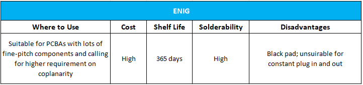
As one of the lead-free surface finishes, the advantages of ENIG are featured with long storage life, good solderability, and flat surface. However, its main disadvantages include that it is comparatively expensive and has the risk of a "black pad."
- Black Pad
A black pad is a defect in solder joints with ENIG applied, which results from serious erosion of the nickel layer. It's called "black pad" as the colors of a damaged nickel layer are grey and black.
The primary drawback of the black pad is that it can't be easily eliminated, and it also cannot be detected by the naked eye, which creates a severe reliability threat to products.
- Disadvantages
a. Non-wettability
Non-wettability is the direct cause of black pad. Generally, a PCB with ENIG that suffers from a black pad cannot stand stress very well. Therefore, products experience fractures in solder joints under high-low temperature cycle tests, vibration tests, and plugging and unplugging every day, thus reducing reliability.
b. Erosion Tendency
The erosion of the solder joints with ENIG may happen under humid conditions due to the thin thickness of the gold layer, which may have pinholes. While gold itself doesn't erode, the layer of nickel underneath is prone to erosion, thus affecting the solder joints.
• Summary
Im-Sn(Immersion Tin)
Im-Sn means immersion tin. The surface finish is formed using a displacement reaction, and the layer is pure tin. Because of this, the thickness of the surface finish is normally limited to 1μm.
- Disadvantages
a. Not Resistant to Storage
The tin layer could diffuse into the copper substrate even at normal temperatures. The tin can hold about 30 days at room temperature, and its diffusion rate is between 0.144 and 0.166 nm/s, however, its thickness would reduce approximately 0.23μm when converting to IMC. After reflow soldering, the thickness can reduce further by more than 0.8μm. If storage for 180 days is required, the soldering has to be done three times such that the Im-Sn minimum thickness is above 1.28μm. However, this is often not achievable by the common thicknesses whose values are around 1.15μm.
b. Color Change
Due to the increase in temperature during soldering, the Im-Sn layer would lead to color change, the reason why is by the organic contaminants or the tin oxidation. In general, the thickness of the tin oxide layer is determined by the darkness of the color.
c. Ineffective for Fine-Pitch Assembly
The tin plating chemical solution adversely impacts most solder masks; hence, Im-Sn cannot be recommended for use in the fine-pitch assembly. The implications are equal to black pad in ENIG. Im-Sn interactions are prone to tin whiskers, while pad spacing exceeding 0.4 mm would avoid this happening.
Via-filled inks may cause topographical damage through the dry film application, which leads to fractures that trap a portion of the chemical solution. Any expelled solution during reflow soldering greatly would impact the final product's appearance and reliability.
• Summary

Im-Ag
Im-Ag is the abbreviation for immersion silver. It is a process in which a layer of silver is deposited on a surface through a chemical solution. The layer is not pure silver, consisting of an organic part, with mass fraction of about 30%.
- Disadvantages
a. Micro Cavities
There are microcavities with a diameter of less than 0.05 mm on the surface of silver, resulting in solder joints having intense damage, further enhanced when the PCB is subjected to mechanical shocks, which may cause defects in the products.
Creeping corrosion is one of the major defects of Im-Ag, which may happen due to galvanic coupling between exposed copper at the edge of the solder mask and the higher surface silver area, eventually corroding in a humid environment.
b. Silver Migration
This is another typical kind of defect that occurs in thick-film circuits or inside the IC.
c. Color Change
An immersion silver layer on the surface of a board will change color to yellow or black after exposure to air, basically because tiny holes on the surface of the silver react with the halogens in the atmosphere, and the surface color can also be different after soldering. Two factors contribute to this color change after soldering: plating thickness and exposure time. Earlier studies have shown that an increase in thickness used during plating also improves resistance to discoloration or helps preserve the color of the surface in applications with short exposure time.
• Summary

OSP(Organic Solderability Preservatives)
Organic Solderability Preservatives are sets of organic film layers created on clean copper through chemical means, which protects copper essentially from oxidation and prevents thermal shock, improving solderability.
- Problems Encountered by OSP After Soldering
Problem #1: Volatilization/ Mass Loss
Under high temperatures in a reflow soldering oven, OSP has little volatilization with a mass loss of not less than 10%. This serves to mean that the thinnest possible layer shall be used for the OSP application.
Challenge #2: Heat Stability
OSP does not decompose up to 260°C, but sublimes, meaning that it could passe directly from the solid into the gaseous state without releasing any heat.
Challenge #3:Reaction with Oxygen
OSP tends to oxidize in the soldering process.
Challenge #4: Discoloration and Deterioration
When OSP is exposed to a soldering oven, it can quickly turn in color to rust, negatively impacting its solderability.
Challenge #5: Difficulties in Removal
OSP may ultimately turn out to be challenging to remove when the flux is applied to it, so stronger flux agents are required to its effective removal.
• Summary

PCBX Ready to Help You with Online PCB Solutions
PCBX is always ready to provide online help regarding your PCB needs. With the comprehensive one-stop solution for PCB fabrication, PCB assembly, and component sourcing, PCBX serves customers with high-quality products at competitive prices, clicking the button below to get the best PCBs for your projects.
Hot Tags:
Contact us

If you can't find what you're looking for, please contact us.
 2024/07/25