- Products & Capabilities

- About
- Resources
Ten Golden Rules of PCB Design


The article is developed concerning the breakthrough of integrated circuits and the need for custom PCBs in some electronic products. It enumerates ten golden rules in conducting PCB layout design and manufacturing: grid selection, routing, power layers, component placement, panel duplication, component value combination, frequent DRC, flexible silkscreen use, decoupling capacitors, and pre-production parameter checks. These rules provide for the optimum design and manufacturing of a PCB.
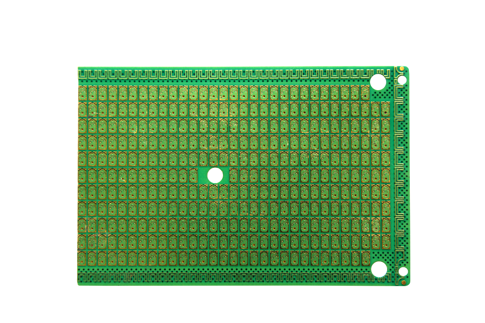
While semiconductor integration is ever-increasing, system-on-chips are still inapplicable for all applications. Ready-to-use boards are powerful and even more easily available; however, many electronic products still demand customized PCBs. Used as the physical design platform and the most flexible part of a PCB in electronic system design for original components, even an ordinary one could play a very important role in one-time development.
The article describes ten golden rules that one should consider while using design software for PCB layout design and commercial manufacturing. Most of those rules remain unchanged since commercial PCB design was invented 25 years ago, making them greatly valuable in guiding electronic design engineers and mature circuit board manufacturers.

Rule 1: Select the right grid set that matches the most components.
Although the multi-grid seems very effective, engineers could avoid problems encountered in the setting of intervals at the early stage of PCB layout design if they had more thought, which could maximize the application of a circuit board. Because many devices use numerous package sizes, engineers should select the product that best fits their design. When polygon copper is used on multi-grid circuit boards, polygon filling deviations are common, not as standard as those based on a single grid but providing more than the required amount of circuit board life.
Rule 2: The route shall be the shortest and most direct.
This might sound simple and common, but it needs to be kept in mind at every stage, even if one needs to change the circuit board layout to optimize the wiring length.
Rule 3: The power layer is preferable to control distribution of the power lines and the ground lines.
The power layer copper typically provides a quicker and easier way in most PCB design software to ensure the current flow with minimum impedance or voltage drop for maximum efficiency by interconnecting wires in common and ensuring sufficient ground return paths.
Rule 4: Keep related components together with their required test points.
Rule 5: Duplicate the target circuit board on a larger circuit board to allow PCB imposition.
The size that best fits the equipment will cut down on the cost of prototyping and manufacturing tremendously. Because the circuit board layout on the panel matters, you need to ask the circuit board manufacturer for their preferred size specification on each panel, then change your design specifications to those and see if you can repeat your design multiple times within these sizes.
Rule 6: Combine component values.
Of course, as a designer, you will choose discrete components with greater or lower values based on component values but behave similarly. More fall within an integrated standard value range, simplifying the bill of materials and lowering associated expenses. If you have a series of items in your PCB line depending on the value of your chosen version of the component, you will be better able to make long-term inventory management decisions.
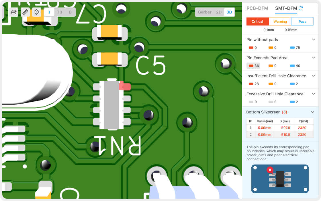
Rule 7: Frequent design rule checks (DRC)
Running the DRC function of PCB software frequently is a good habit. It takes little time, but it saves a lot of time even in a more complicated design environment, as long as you always check while designing.
Rule 8: Use silkscreen flexibly.
Silkscreen can be used to mark useful information for circuit board manufacturers, service or test engineers, installers, or equipment debuggers. Not just clear function and test point labels; after the circuit board has been assembled, you can also indicate the direction of components and connectors wherever possible with these comments printed on the lower surface of the components used on the circuit board. The entire application of silk screen technology on the upper and lower surfaces of the circuit board helps avoid repetitive work and, hence, makes things easier in the process.
Rule 9: Selecting the decoupling caps.
Do not try to optimize your design by avoiding decoupling the power lines based on the limit values in the component datasheet. The capacitors are inexpensive and long-lasting. You can afford to spend as much time as possible assembling the capacitors. To keep your inventory neat, follow Rule 6, which states that you should use the standard value range.
Rule 10: The PCB parameters must be checked before submitting for production.
Although most circuit board manufacturers download the uploaded files directly to verify the parameters, it is still better to output the Gerber file by yourself and verify it with a free viewer to reduce the risks of misunderstandings. You may even find some negligent errors and avoid losses caused by production according to the wrong parameters.
Hot Tags:

Contact us

If you can't find what you're looking for, please contact us.
Article
IC packaging is essential in electronics for protecting components, providing electrical connections, and managing heat. This tutorial explores its complexities, including its importance, various types like SMD, QFP, and BGA, and considerations for choosing the right package for specific applications. Proper IC packaging enhances PCB performance and reliability.
 2024/09/12
Designing a PCB involves ten detailed steps: schematic capture, creating a blank PCB layout, syncing designs, defining stackup, setting design rules, placing components, adding drill holes, routing traces, labeling, and generating output files. These steps ensure an organized, error-free process from concept to manufacturing.
2024/08/29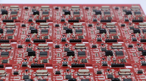
Thermal management is all about more than just keeping the temperature of electronic systems and printed circuit boards low. It has been a key issue related to reliability and performance. Of the very basic fundamentals that would be studied in the field, some are concerned with methods of heat transfer. These are through conduction, convection, and radiation. The methods of cooling include natural cooling, forced-air cooling, fluid cooling, and evaporation cooling. Appropriate thermal design rules shall be followed wherein the chosen materials provide optimum thermal conductivity and the components of a system are so laid out that no hot-spotting will take place. Thermal analysis becomes critical in pointing out heat-related issues and optimizing the design. It thus minimizes failure rates and enhances stability and functionality of the electronic systems through comprehensive thermal management.
2024/07/25