- Products & Capabilities

- Simulation Design & EDA

- About
- Resources
What's Next for PCBs?丨Future Of PCBs


The article explains the current situation of Printed Circuit Boards and future development based on efficient production helped by advanced software and manufacturing processes. Future technological developments are in store for 3D Printed Electronics, flexible PCBs, eco-friendly biodegradable PCBs, and board cameras. It elaborates on other powerful automation tools that are going to make the entire PCB design process efficient in the near future. All of them will further improve and develop with the technological advances in PCBs, keeping up with the ever-increasing industry and consumer demands.
From their invention in the early century to their patenting by Paul Eisler in 1943, printed circuit boards have advanced beyond their original functionalities.
Today, PCB is a tiny, multilayered, and complex system, barely resembling its prototype. They are also fabricated in much larger quantities and more effectively than ever before, due to sophisticated design software and manufacturing processes. Microvias, HDI, and FPGAs that were only used in the most costly designs 10 years ago are readily available worldwide.
As technology and consumer demand grow and develop, however, so must PCB. PCB, the foundation for all electrical devices, is under constant development pressure. With consumers pushing for slimmer and faster devices and industries seeking improved functionality, PCB has to keep developing in the future.
What will the Future of Printed Circuit Boards Be Like?
Future of Printed Circuit Board
Even though PCBs are fabricated today in incredible volumes with astounding complexity, there is always room for improvement. Be it in the shape of the PCB itself or the assembly affixed directly to the board, consumers are constantly demanding new and different PCBs and PCB functions.
There is also plenty of space for expansion in the manufacturing process, as the rising complexity of PCBs presents new problems for manufacturers. Thus, most predictions made for the future of the printed circuit board focus strongly on the following areas.
PCB Board Cameras
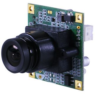
A board camera, also known as a PCB camera, is mounted directly onto a circuit board, with a lens, aperture, and image sensor designed to capture digital pictures or videos. Overall, this camera is about the size of a quarter and can be put on any PCB, which makes the camera small enough to slip into just about any electronic device.
Board cameras have developed fast since their invention. Two primary areas for development are photo and video imaging, along with durability. Nowadays, these tiny cameras can easily capture high-resolution images and videos. In the coming years, board cameras are predicted to move further on the path of development, building up a strong solution in both industry and consumer electronics.
Due to their small size, board cameras have several applications across different industries, including:
• Consumer Electronics: Board cameras have found a great deal of utility in consumer electronics, particularly in handheld mobile devices. Today, all smartphones, tablets, and laptops come fitted with board cameras. In the future, consumer electronics companies will continue to push even smaller and more powerful cameras.
• Medical Devices: Especially small board cameras have been widely applied in the field of non-invasive and minimally invasive procedures. Today, there is the availability of pill-sized cameras that patients can swallow to let doctors take thorough videos and images from inside the digestive tract without needing invasive surgery. Meanwhile, wearable cameras are becoming popular during surgeries as an instructional tool.
• Surveillance Technology: Because the PCB camera is very small, it can easily be inverted inside an object, thus becoming a great tool for surveillance purposes. Several customers, like security agencies and institutions, use these minimal cameras for monitoring their houses and offices to avoid intrusion. The more technology develops, the more its applications in surveillance grow.
These industries are examples of the usage and trend of board cameras. As it now stands, the application of board cameras is shifting more into customizable board cameras that are high in quality and durable, and better day/night and low light capabilities are underdeveloped to achieve both medical and surveillance imaging purposes.
3D Printed Electronics
3D printing technology is probably one of the most exciting technological innovations in recent years. With this technology, anything from organs to firearms and ammo is possibly finished in an extremely short period across multifarious industries, so as PCB.
3D printing thus plays a key role in recent PCB innovations: the 3D PE. 3D-printed electronics, also called 3D PEs, hold great promise in changing the appearance of electrical systems design, by printing a substrate item layer after layer to make three-dimensional circuits. Therefore, liquid ink with electronic functionalities can be added, and surface-mounted technologies can be added on top to constitute a final system. The form of the circuit can be any shape. 3D PE can offer enormous technical and manufacturing advantages for circuit vendors and their clients — much more so when compared to traditional 2D PCB. The advantages include:
• Novel Designs: Allowing circuits to be directly printed on top of an existing shape, 3D PE manufacturing techniques make circuits realize new and incredible shapes, impossible to achieve with the traditional methods of PCB manufacturing. 3D PE can be shaped to any circuit carrier while combining the most important electronic, optic, and mechanical functions, which allows new product features and optimizations. Not only can 3D PEs be shaped, but they can also be scaled to print on components larger than anything possible with the manufacturing methods of 2D PCB.
• Better Efficiency: As 3D PE manufacturing is an additive process using digital methods, it is much more conservative in its materials usage compared with traditional 2D PCB manufacturing. Because it applies only the quantity of material required, the materials will be better utilized. Moreover, the digital part of the production process increases accuracy owing to human error that can be eliminated. Although this method still occasionally fails a circuit, increased automation does lower this likelihood, therefore increasing its overall efficiency.
• Environmentally Friendly: 3D PE manufacturing puts no limitation on the type of substrate material to be used by a PCB House, so it makes selecting materials easier for environmentally friendly production since they can easily choose low-cost and recyclable materials.
It is because of the above advantages that 3D PE production has rapidly progressed and is heading toward high-volume mass production. Though 3D PE applications are relatively few at this time and largely remain with gauges, antennas, and sensors, a lot of research is currently being put into developing 3D PE manufacturing capabilities, including developing surfaces that they can be printed on, SMDs that can be added to them, and the manufacturing tools that can be used to print them.
Considering this, many industry leaders believe that 3D PE is bound to grow fast as more and more manufacturing companies and consumer industries come up with new techniques and uses for this kind of technology.
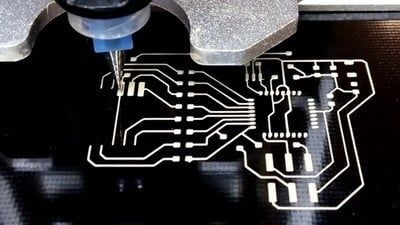
PCB Autoplacers
Most of the present PCBs come complete with an auto-router as part of their design. The electronic functions around a board are used to model the characteristics of the laid-out PCB, hence greatly easing the automation process.
However, setting up and creating an auto-router is difficult and time-consuming; because of this, it would lose setup time which gained in automation. Under this circumstance, many manufacturers and PCB designers regard autoplacers as an alternative. Autoplacers make the automation process considerably faster by attempting to integrate mechanical and electrical CAD systems which in turn simplifies the manufacturing process. Up to now, the reason why automatic placement tools haven't been accepted in the PCB manufacturing industry at large lies primarily in the difference between auto placer and auto router constraints:
• Autorouters: A lot of the board characteristics, like numbers of layers, track separations, distances between the connections, and directions of the layers, drive most of the routing constraints and are easily modeled in a PCB design environment.
• Autoplacers: Driving constraints to the component placement can be mechanically based, including the shape of the product casing, ergonomic issues such as button position, heat dissipation, and pick-and-place optimization.
The constraints that govern how autoplacers operate are often unrelated to the board design itself, but to product design, which lets designers be concerned with so much more than the actual design of the PCB, such as the extremely high new cost. Autoplacers can crank up the speed in manufacturing compared to autorouters; however, this is mainly dependent on the level of optimization done in the autoplacer constraint management. That is where new technology needs to step in.
With the innovations in PCB design technology, the ideas of integrated CAD systems also come to the fore. In this way, since auto placers depend on both electrical and mechanical design aspects, an electrical-mechanical integrated CAD system that applies constraint management into both realms is necessary to get at making the auto placer more efficient.
With these design software trends, the auto place is becoming the more efficient replacement for autorouters, therefore, the shift from autorouters to autoplacers is likely to become truly helpful in the PCB design process.
High-Speed Capability
The world is developing at a superb pace, which compels people and technology to move fast as well. But looking through the development in recent years, we have been expecting things to get even faster—with no exception for electronics, in particular. For our devices to get ahead in this ever-growing increase in speed, the technology of PCB will have to adapt correspondingly.
High-speed PCB is a unique subject for designers mostly because its definition is relatively loose. The generally agreed definition of a high-speed PCB would therefore be one where the integrity of the signal is affected by the diagram of the circuit layout. That will give rise to different meanings:
• Digital Signal: The intelligence in digital PCB signals is stored in digital pulses, so effects on the integrity of signals are shown as being delayed or canceled.
• Analog Signal: In a Hs analog circuit, the shape of the signal is intelligent. Indeed, SI issues raised would express themselves through changes in the signal shape.
In both cases, several factors can have a negative impact on signal integrity either inside or around the PCB, including the PCB dielectric, track length, and distance to other signals and EMI, amongst others. Most high-speed designers know how to tweak designs to prevent these problems from happening in the first place, but there are always new methods under development as well as new software tools to manage high-speed designs.
Want to learn more about the current high-speed PCB design technique? Please check out pcbx.com for Resources on PCB Design and read our articles on High-Speed Layout Tips and How to Reduce EMI Influence in High-Speed Designs.
Given the expectation of continued high demand for high-speed functionality, the emphasis on Printed Circuit Board developments that cater to high-speed designs is likely to remain strong. According to PCB industry experts, high-speed developments will play a significant role in the board's future.
A Focus on Flexible PCB
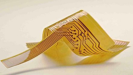
The PCB industry itself is fast-growing, with a constant grow from $63.5 billion in 2016 to $73.8 billion in 2021. Flexible PCB, however, is the sector of the PCB industry growing at a faster-than-usual pace. This growth—contrasted with the PCB industry, increased by up to $15.2 billion in 2020 and $27 billion in 2022.
From wearable electronics and flexible displays to medical applications, flexible technology is driving the industry evermore in a flexible and flex-rigid direction. Flexible PCB technology already outclasses its rigid counterparts in yearly sales growth, so things look auspicious for it in the future.
The reason for the very wide popularity of flexible PCB is mainly for their flexibility. Taking more stress and bending than rigid PCB, the flexible one can even be folded up to fit into three-dimensional spaces, making them quite helpful for applications in which bending is a regular occurrence. They are usually very light and thin, but ensure the ease of production in bulk.
Several industries are driving this trend toward flexible PCB, including:
• LED Lighting: LED lighting proves widely used as the substitute for traditionally incandescent bulbs, bright yet efficient. Flexibility is necessary along the length of LED strip lighting so that consumers can bend it to meet their demands. In this regard, flexible PCBs provide the necessary functionality.
• Wearable Technology: Today, wearable electronic device usage is getting ever more popular, with the global market reaching $30.6 billion by 2020. Quite often, the space contains these electronics, which have been embedded into clothes and flexible accessories such as socks, belts, and wristbands. Others have fitted some of their sports helmets with additional sensors using PCBs that will not only track shock but also speed. All these require flexible PCB, not only for flexibility but also for shock and vibrations.
• Flexible Displays: Flexible displays have sparked interest for years, but they are still uncommon and are not widely used because of their high production costs. However, when those production costs come down, flexible devices become the next big thing in mobile technology. Capable of withstanding shocks and stresses more than regular rigid designs, flexible displays would facilitate the improvement of flexible smartphones and tablets. This will likely require everything else in the device to be bendable, PCB as well.
• Medical Instrumentation: Innovation in medical devices so far has focused mostly on two trends in technology: miniaturization and flexibility. Flexible PCB could make medical devices achieve both by creating compact circuitry on a flex substrate. Moreover, flexible PCB is favored due to their reliability and biocompatibility of the substrates, which make them compatible with human tissues, down to their constant connections. For such, flexible PCB has already become a mainstay in a lot of medical devices applied in surgical tools, implantable medical devices, monitors, and sensors.
Flexible PCBs are in high demand because of their literal and metaphorical flexibility, which allows for a wide range of applications across sectors. If this trend continues, people in the PCB sector should expect a surge in demand for more flexible PCB designs.
Biodegradable PCB
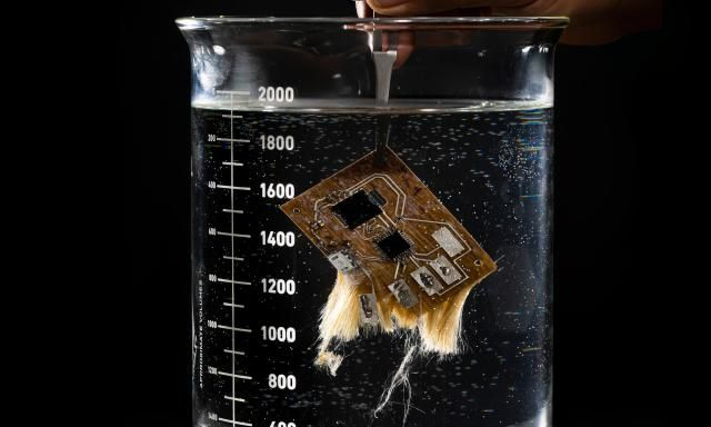
Electronic waste, also called e-waste, is one of the biggest environmental concerns in the modern era, including computers, laptops, TVs, smartphones, and house appliances, many of which are made with parts that are not biodegradable or friendly to the environment. While e-scrapping has evolved in recent years, e-waste continues to be a problem as people try to find ways to get rid of old electronics.
Much of it is part of the problem of PCB. Some PCB materials do not degrade easily and often find their way into landfills, potentially contaminating the land around them. That problem is confounded by the fact that such chemicals used in processing the materials for making the PCB could be hazardous to the environment on disposal.
Given how many electronics the average consumer uses in a decade and the industry's trend toward short-lived electrical items, many discarded PCBs may harm the environment.
The solutions proposed for the situation range from mass junking to organized e-waste collection services, with some even advocating for the extraction of precious metals from e-waste, such as palladium, silver, gold, gallium, and tantalum, for reuse through smelting and refining, thereby reducing the pressure on mining companies to produce large amounts of metal for use in electronics.
What some scientists recommend that the problem of the level of pollution by replacing the manufacturing processes involved in making the PCB, which calls for new substrates that are more environmentally friendly than the traditional ones. Biodegradable substrates have been scrutinized along with those finishes that do not use harmful etching chemicals to complete the assembly process.
Both would contribute to the reduction of the environmental impact of the electronics industry as a whole and may help bring down the cost of assembly and manufacturing.
Other Future Advancements in PCB Industry
The improvements and innovations in the PCB industry are listed above. Many other potential innovations lie just beyond the technological horizon.
Current trends show that the work of the PCB is to connect electronics, passing messages from one component to the other for the device to work, which would make PCB an active system, reducing the amount of components while maintaining functioning.
Other advances deal with the interface between these innovations. For example, 3D PE manufacturing is increasing the kinds of materials that can be used for circuits, making the ability to use flexible and biodegradable substrate materials more plausible. Utilizing the integration of these new innovative ideas, designers can do amazing ground-breaking new designs that keep the technology of the PCB moving forward.
Choose PCBX for Your Future Projects
The technology of PCB continues to evolve well into the future—with customers' needs and priorities changing. When your business works on new designs and new technologies, including the above trends, you will also need to find a partner in PCB solutions ready to adapt to changeable technological requirements far into the future. That is where the help of PCBX comes into the picture.
PCBX is dedicated to providing the best solution for partner companies to source parts and PCB assembly. We will be there to help you through each stage of your PCB fabrication and assembly process. With almost 20 years of experience, PCBX will give you comprehensive professional service. Our assembly adheres to IPC Class 3, RoHS, and ISO 9001:2008 certification standards and is set to handle even the most complex PCB designs. No matter what you need, PCBX is always there to help.
To learn more about PCBX and how we will serve your next project with printed circuit boards, please request a free quote today for standard PCB, PCB prototype, or assembly services.
Hot Tags:

Contact us

If you can't find what you're looking for, please contact us.
Article
SMT has transformed electronics manufacturing by enabling automation and miniaturization, leading to more efficient assembly processes and the production of high-quality, compact electronic devices.
 2024/10/14
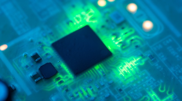
PCBs are essential for organizing information and power flow in electronic devices, benefiting from flexibility, durability, safety, efficiency, and heat management.
2024/08/13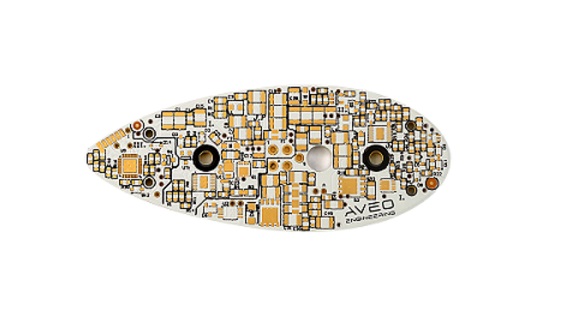
Aluminum PCBs are widely used electronic boards with comparatively better heat dissipation properties. The aluminum core cools down the components of the product, thereby improving its performance. These are eco-friendly, light, and strong PCBs and hence appropriate to be used in audio equipment, power supplies, and lighting products such as LED lighting.
2024/07/24