Altium Design Tutorial
A Complete Design Tutorial with Altium Designer
In this tutorial, I'll guide you through the process of quickly and easily designing PCBs for your DIY projects using Altium Designer.
Altium Designer is a powerful and versatile tool that allows us to take our DIY projects to the next level. With its user-friendly interface and comprehensive feature set, we can seamlessly translate our circuit schematics into high-quality PCB designs, ready for manufacturing.
By the end of this tutorial, you'll have the knowledge and skills to efficiently design and produce PCBs for all your future DIY projects, taking your creations to new heights. Let's dive in and explore the world of PCB design with Altium!
Altium Tutorial Step 1 – Download Altium Designer

Here are the steps to download Altium Designer:
Visit the Altium Website: Go to the official Altium website at https://www.altium.com.
- Navigate to the Download Page: At the top of the homepage, click on the "Products" tab and select "Altium Designer" from the dropdown menu. This will take you to the Altium Designer product page.
- Click on the "Free Trial" Button: On the Altium Designer page, look for the "Free Trial" button and click on it. This will initiate the download process.
- Fill Out the Registration Form: You will be prompted to fill out a registration form with your personal and contact information. This is required to create an Altium account and access the free trial.
- Choose Your Operating System: Select the appropriate operating system (Windows or macOS) for your computer. The download file will be tailored to your selected OS.
- Download the Installer: Once you've completed the registration form, click the "Download" button to begin downloading the Altium Designer installer file to your computer.
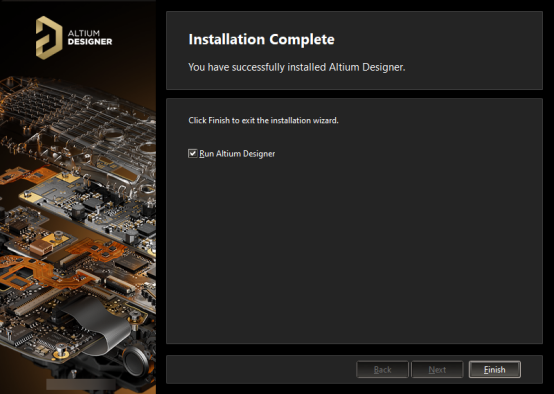
- Run the Installer: Locate the downloaded installer file and run it. The Altium Designer installation wizard will guide you through the installation process step-by-step.
- Activate the Free Trial: During the installation, you will be prompted to activate your Altium Designer free trial. Follow the on-screen instructions to complete the activation process.
That's it! Once the installation is complete, you'll have full access to Altium Designer and can start designing your custom PCBs for your DIY projects.
Altium Designer is a powerful and user-friendly PCB design software. It offers a wide range of features that make the design process efficient and collaborative. Some key benefits of Altium Designer include:
Centralized Cloud Storage: Altium provides cloud-based storage that allows you to access your design files from anywhere and collaborate with team members in real-time.
Online Collaboration: The software enables seamless online collaboration, allowing you to share your PCB designs and ideas with your network.
Hobby and Professional Use: Altium Designer is suitable for both hobbyist projects and professional PCB design. You can use it to design and create custom PCBs for your personal projects.
Free Trial and Student License: Altium offers a free trial version that you can download and install. Additionally, students can get a 6-month full license for free, which is an excellent opportunity to explore the software's capabilities.
To get started, simply visit the Altium website and download the free trial version. Once downloaded and installed, you can open the software and begin designing your PCBs. The user-friendly interface and powerful tools within Altium Designer will help you bring your ideas to life, whether you're a hobbyist or a professional.
1.Start a New Project in Altium Designer
Launch Altium Designer: Open the Altium Designer software on your computer.
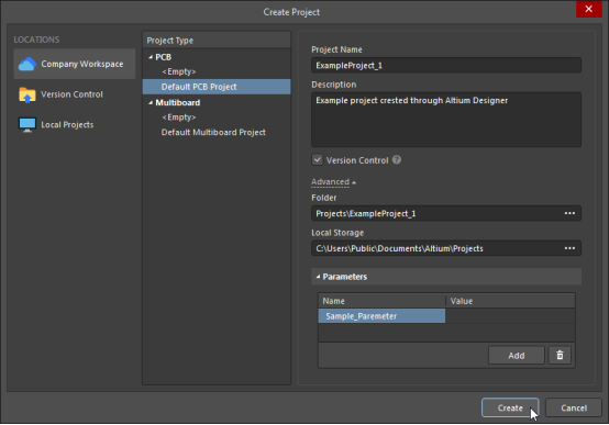
Create a New Project: In the welcome screen or the main menu, select "File" > "New" > "Project". Alternatively, you can click the "New Project" icon on the toolbar.
Choose a Project Template: Altium Designer provides several project templates to help you get started. Select the one that best suits your needs, such as "Basic PCB Project" or "Schematic and PCB Project".
Name and Save the Project: In the "New Project" dialog, provide a name for your project and choose a location to save it. Then, click "OK" to create the new project.
Set Project Preferences: Altium Designer will open the new project. You can now set various project preferences, such as the default design rules, design layers, and output settings. You can access these settings by navigating to "Design" > "Project Preferences".
Create a Schematic: If your project includes a schematic, you can start by creating a new schematic document. Right-click on the "Schematic Documents" folder in the Projects panel and select "Add New To Project". This will open a new schematic sheet where you can start placing and connecting components.
Design the PCB: Once you have the schematic ready, you can create a new PCB document by right-clicking on the "PCB Documents" folder in the Projects panel and selecting "Add New To Project". This will open a new PCB editor where you can start placing components, routing traces, and designing the layout of your PCB.
Save and Manage the Project: As you work on your project, be sure to save your changes regularly. You can also use the Project panel to manage your project files, such as adding new documents, importing libraries, and organizing your design.
2. Place schematic parts

Now let's place our first component. Simply search for the component you want to add and you should see a list of all available options. Check the details and footprint of each one to make sure you select the right one.
Once you've found the component you want to use, add it to the circuit. To do this, right-click on the component and select "Place". Your cursor will change to indicate you are in placement mode. You can then click anywhere on the schematic to place the component.
1) . Open the saved schematic file you want to work on.
2) . On the left side of the screen, click on the "Libraries" bar. This will open the Libraries panel, where you'll see all the components available for your design.
3) . Select the components you want to use from the Libraries panel. Once a component is selected, click the "Place" button to add it to the white drawing area on the right side of the screen. You can then rotate or orient the component as needed for your design.
Click on the Tools bar, which will reveal a variety of tools you can use to modify your schematic. Take a look through the available tools and select the ones you need for your schematic design.
3. Update the PCB from the schematic
1).After making your modifications to the schematic, it's time to update the PCB document from the schematic. To do this, go to the Design menu and select "Update PCB Document".
When the Engineering Change Order dialog appears, click "Validate Changes" first. Once that's complete, click "Execute Changes".
When you see green checkmarks appear next to the "Check" and "Done" columns, it indicates there are no issues with your schematic design and the update to the PCB was successful.
4. Board Shape and Layer
Circuit board design should be completed within a specific boundary, so the board shape must be redefined. To do this, go to the Design menu and select "Board Shape" > "Redefine Board Shape".
PCBs typically have multiple layers. When designing a custom PCB, you'll need to define the specific layer for each component. To do this, go to the Design menu and select "Layer Stack Manager".
If a component is placed on the bottom layer of the PCB, double-click the component in the design to open its properties. Then, set the "Layer" property to the appropriate bottom layer. This will update the layer information shown in the PCB design graphic.
5. Rules and Routing
(pic from Altium Design)
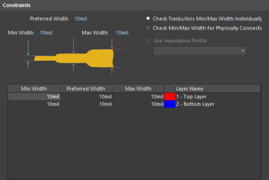
1.To define design rules, go to the Design menu and select "Rule...". This will allow you to choose the different types of rules you want to apply to your PCB design.
2.To automatically route the connections on your PCB, click the "Auto Route" button, then select "All...". This will initiate the auto-routing process.
3.While the auto-routing feature can be convenient, it may not always produce the best results. For more control over the routing, you can use the "Interactively Route Connections" tool. This will allow you to manually route the connections as desired.
6. Mounting Holes and File Generation
Locate the yellow hole indicator on the top of the PCB design.
Double-click on the yellow hole to open its properties. Here, you can customize the hole size, shape, net connection, and other relevant settings.
To add a text string to your PCB, go to the Place menu and select "String".
AD File Generation
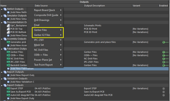
(pic from Altium Design)
1.Prepare the PCB Design:
Ensure your PCB design is fully complete and ready for manufacturing.
Verify that all components have been placed correctly.
Confirm that all necessary routing has been done.
Review the overall design to ensure it is ready for output and fabrication.
2.Navigate to the Output Job File:
In Altium Designer, locate the "PCB" panel.
Right-click on the PCB file you want to generate Gerber files for.
From the context menu, select "Output Job File".
3.Configure the Output Job File:
In the "Output Job" window, you will see a list of predefined output options.
Expand the "Fabrication" section.
Select the Gerber outputs you need, such as:
- Top Layer
- Bottom Layer
- Solder Mask
- Silkscreen
and any other necessary Gerber files for your PCB manufacturing.
4.Review and Customize Gerber Settings:
- In the "Output Job" window, double-click on each Gerber output item in the list.
- This will allow you to review and customize the settings for that specific Gerber file.
- Verify that the layer name, file type, and any other relevant parameters are correct and match your PCB design requirements.
5.Set the Output Folder:
In the "Output Job" window, locate the section where you can specify the output folder.
Determine the appropriate location where you want the Gerber files to be generated.
Enter or browse to the desired output folder path.
Choosing the correct output folder is important, as this is typically the location where you will send the generated Gerber files to the PCB manufacturer for the fabrication process.
7.Generate the Gerber Files:
- After reviewing and configuring all the necessary Gerber outputs in the "Output Job" window, locate the "Output Job" button at the bottom of the window.
- Click the "Output Job" button to initiate the generation of the Gerber files.
- Altium Designer will now generate the Gerber files and save them in the specified output folder.
8.Additional Files:
Depending on your preferences or the manufacturer's requirements, you may need to generate additional files alongside the Gerber files, such as:
- Drill Drawing (NC Drill)
- Drill Guide
- Assembly Drawings
- Bill of Materials (BOM)
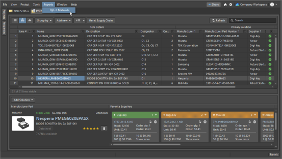
(pic from Altium Design)
These supplementary files can provide the manufacturer with further details and information required for the complete PCB manufacturing process.
Ensure that you review the manufacturer's requirements and generate any additional files that may be necessary for a successful PCB fabrication.
Conclusion:
Up to this point, you have completed the core aspects of your PCB design. The functionality demonstrated in this tutorial covers the basic range of capabilities within Altium Designer.
As you become more proficient with Altium Designer, you will discover a wide range of advanced tools, workflows, and design capabilities that can be leveraged to create more complex and sophisticated PCB designs. The depth and breadth of Altium Designer's functionality is expansive, allowing you to continuously refine and improve your PCB design process.
The key is to continue learning, experimenting, and applying your knowledge to unlock the full potential of Altium Designer for your specific PCB design needs.