How to generate PCB Gerber files in Altium?
Ready to send your Altium Designer PCB design off for fabrication? The key step is generating accurate Gerber files that the manufacturer can understand. This guide walks you through the process step-by-step, ensuring you provide all the necessary information for a smooth production run.
- Accessing Gerber File Generation:
- Open your PCB design in Altium Designer.
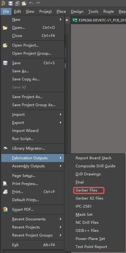
- Navigate to the File menu and select Fabrication Outputs.
- Choose Gerber Files from the drop-down menu.

2. Configuring Gerber File Settings:
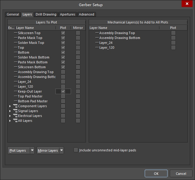
The Gerber Setup window allows you to define how your PCB data translates into Gerber files. Here's what to configure:
- Layers Setting:
- Ensure a clear mechanical layer outline is present. This defines your board's physical shape.
- Select "**Select Used**" in Plot Layers to include only the necessary layers for fabrication. These typically include:
* Copper Layer(s)
* Solder Mask Layer
* Silkscreen
* Paste Layer(s) (if applicable)
* Mechanical Layer
* Drill Drawing
* Drill Guide

- Leave other settings at default and click **Apply**.
3. Generating NC Drill Files:
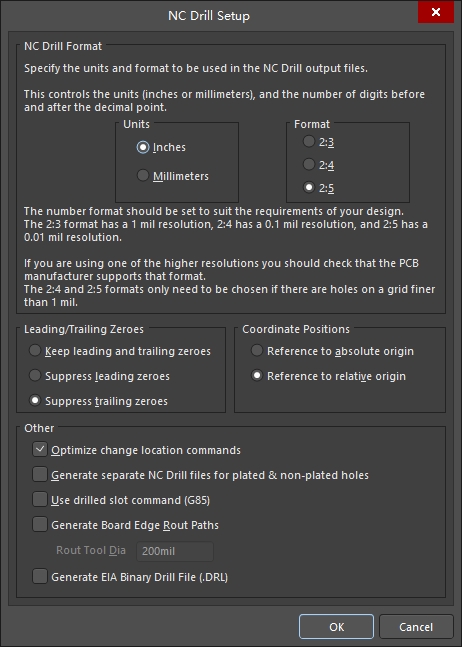
- Drill information is crucial for accurate hole placement. Here's how to create the NC drill files:
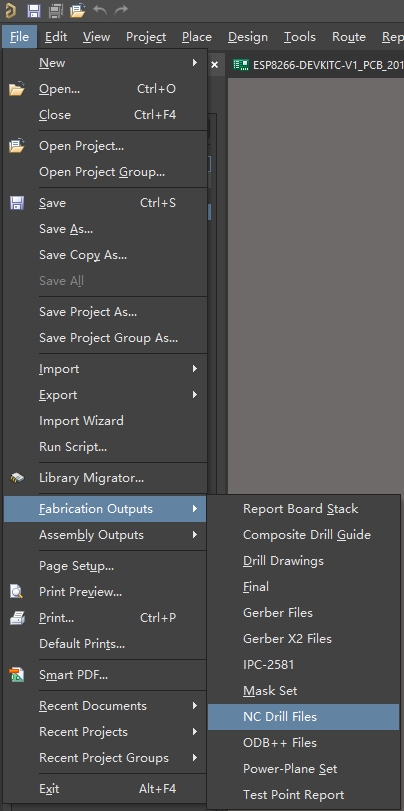
- Go to File > Fabrication Outputs > NC Drill Files.

- Set the precision to 2:5 (0.01 mm resolution). Click OK.

