E-Test
What is E-test in PCB?
E-testing is the essential final step in PCB manufacturing, acting as a quality checkpoint by using electrical probes to meticulously examine bare boards. This inspection ensures the board meets its intended electrical specifications by searching for defects such as shorts, opens, and incorrect resistance or capacitance values. By catching these issues before components are added, E-testing prevents costly rework and guarantees high-quality, reliable PCBs.
Imagine building a house without checking the electrical wiring first, which is essentially what skipping E-testing during PCB manufacturing would be like.

Types of E-test
Moreover, we all know that E-testing uses a blueprint (netlist) to check a bare PCB's connections. Any mismatch between the plan and reality means potential trouble. Generally, there are 2 methods of doing an E-test.
- Flying Probe: Flexible probes move across the board, making contact with various test points.
- Nail Fixture: The board is placed in a specialized fixture with pre-defined test points.
- Manufacturers may assure high-quality PCBs by implementing E-test, avoiding costly rework and ensuring reliable electronics.
FPT
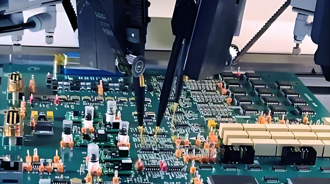
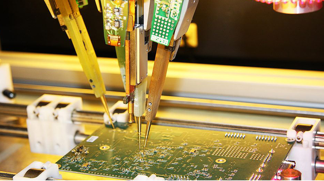
The flying probe test (FPT) refers to the process of testing electronic printed circuit board (PCB) during manufacturing using probes that "fly" to the test points.
A flying probe tester utilizes one or more test probes. These probes can contact test points on the circuit board from both the top and bottom sides, then moving from one position to another on the board to test multiple traces or components.
They operate according to a program that outlines the specific circuit board being tested. These machines use high-precision needles to ensure the PCB functions properly. These systems do not require any test fixtures or custom tools. The probes have virtually no restrictions in accessing the circuit board and can test boards with numerous traces, which makes flying probe testing a cost-effective option for boards in the early development stages. FPT is also very well-suited for low to medium-volume production.
Many consider flying probe testing the most proven method for testing printed circuit boards.

Advantages and Disadvantages of FPT
Advantages:
- Cost-Effectiveness
A more cost-effective approach, especially for testing small-scale production runs.
- Lower Initial Costs
FPT does not incur expenses associated with test fixtures.
- Suitable for Small to Medium Production
Due to its low development costs and short development time, flying probe testing is very suitable for low-volume production.
- Greater Flexibility
Despite some limitations with more complex tests, this method is still beneficial and flexible.
- Accuracy and Precision
Test probes can be precisely positioned and offer a high level of accuracy and reliability. The precision of flying probes helps prevent issues in the final product.
- Short Development Time
The run time for flying probe tests varies depending on the size of the board. In most cases, the test time per board is approximately 5-15 minutes.
- High-Tech Features
Flying probe testing includes high-tech features such as phase difference measurement (PDM) units and micro-short circuit detection.
- Fewer Custom Tools
Flying probe testing does not require custom tools as in-circuit testing does, reducing initial costs and startup time.
- Optimal Inspection
Due to its high accuracy, you can combine flying probe testing with automated optical inspection (AOI) to verify the correct formatting and placement of each part on the printed circuit board.
Disdvantages:
- Flying probe tests may leave small dents in the solder, raising cosmetic defect concerns.
- Probes might miss poorly soldered components by contacting non-pad areas.
- Double-sided PCBs require flipping for testing, preventing simultaneous top and bottom inspection.
Nail Fixture
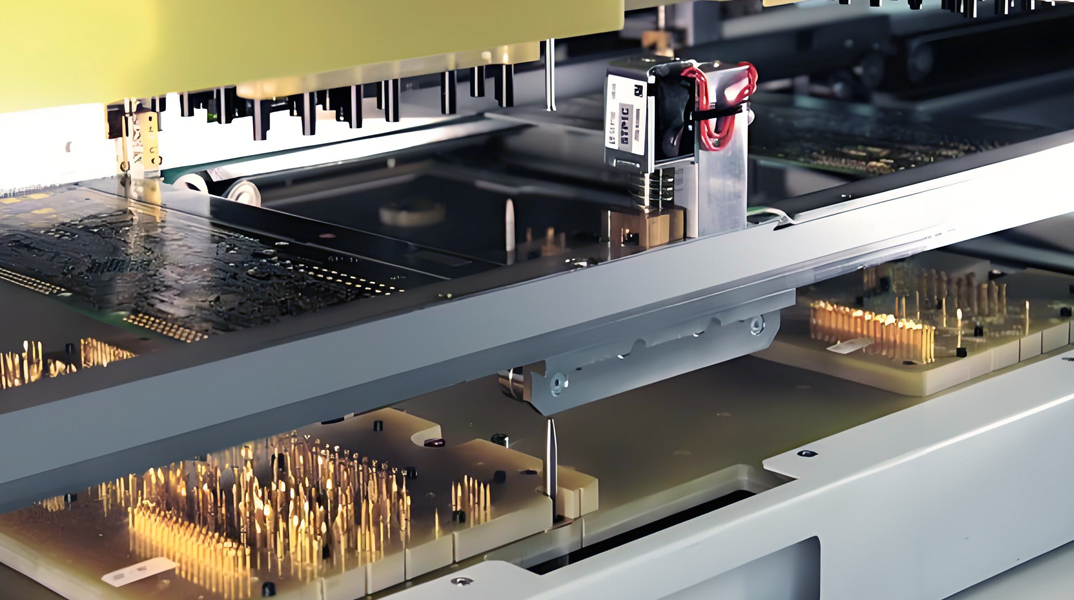
Nail Fixture is one of the PCB testing method, using a template with pins aligned to test locations. Pogo pins are inserted into a laminated sheet to create the template. Testing involves pressing the board against the fixture for instant verification of stable connections. While setup is time-consuming and costly, the method allows rapid testing for mass production.

The fixture aligns nails precisely with test nodes and other circuit features for in-circuit testing. During testing, the PCB is placed on the fixture, allowing pins to establish electrical connections. Dedicated hardware and software are used for continuity checks, fault isolation, and circuit validation according to the test plan. The fixture enables efficient testing by providing access to multiple nodes simultaneously.
Advantages and Disadvantages of Nail Fixture
Advantages:
- High-Efficiency Rapid Testing: Enables quick testing of many PCBs after setup, ideal for mass production.
- Simultaneous Multi-Node Testing: Allows multiple test nodes to be accessed at once, enhancing efficiency.
- Stability and Reliability: Ensures stable and precise connections with accurate pin alignment.
- Versatile Testing Capabilities: Supports continuity, short-circuit, open-circuit, and component functionality testing.
- Reduced Human Error: Minimizes the need for manual intervention, reducing the chance of errors.
Disdvantages:
- High Initial Cost: Expensive to manufacture and set up, especially for complex PCBs.
- Long Setup Time: Time-consuming initial design and setup, not suitable for small or frequently changing batches.
- Lack of Flexibility: Limited to specific PCB models or designs, inconvenient for frequent design changes.
- Complex Maintenance: Requires regular maintenance and probe replacement due to wear and tear.
- Large Space Requirement: It needs substantial storage and operating space and is not ideal for small environments.
Key Differences Between Nails Fixture and FPT
| Categories | Nails fixture | Flying probe |
| Fixturing requirements | Expensive, custom fixtures per design | Cost-effective, universal fixture with adaptable probes |
| Test point access | Parallel access to numerous test points | Sequential probing with limited parallel channels. |
| Programmability | Fixed test points, requiring physical modification | Flexible test points, modified via software |
| Board handling | PCB stress, potential damage | Gentle probing, minimal PCB stress |
| Test types and capabilities | Comprehensive testing, complex diagnostics | Basic testing, limited diagnostics |
| Throughput and volume | High-speed, high-volume testing | Moderate-speed, flexible testing |
| Cost considerations | High upfront costs, low per-unit costs (high volume) | Low upfront costs, high per-unit costs |
Conclusion
Choosing the appropriate E-Test method depends on production volume, testing requirements, budget constraints, and flexibility needs. For high-volume and stable designs, nail fixture testing offers unmatched speed and efficiency. For smaller volumes, frequent design changes, and lower initial investment, flying probe testing provides flexibility and cost-effectiveness.
However, both E-Test methods have their unique strengths and are indispensable in ensuring the delivery of high-quality PCBs. Leveraging the appropriate testing technique enhances the reliability of electronic products and reinforces their performance in real-world applications.


