

Free DFM Check
Along with our PCB Assembly Service, we offer Free PCB File Check or Free DFM (Design for Manufacturability) by checking your PCB design files for any problems that will delay or trouble the manufacturing process. If there are any problems, we will notify you right away by email and work with you to correct the issues and adjust the fabrication schedule of your PCBs as necessary.
Though this is a free service, the DFM Check at PCBX is beneficial because we use the Valor DFM/DFA checking system, to quickly detect any manufacturing problems that may interfere with your PCB manufacturing process, which benefits your production by cutting costs and delivering your PCBs in a shorter period.
PCBX will conduct DFM checks from five aspects: Drill Checks, Signal and Mixed Layer Checks, Power/Ground Checks, Solder Mask Checks, and Silkscreen Checks. The detailed checklists are as outlined below, for PCB DFM checks.
Drill Checks
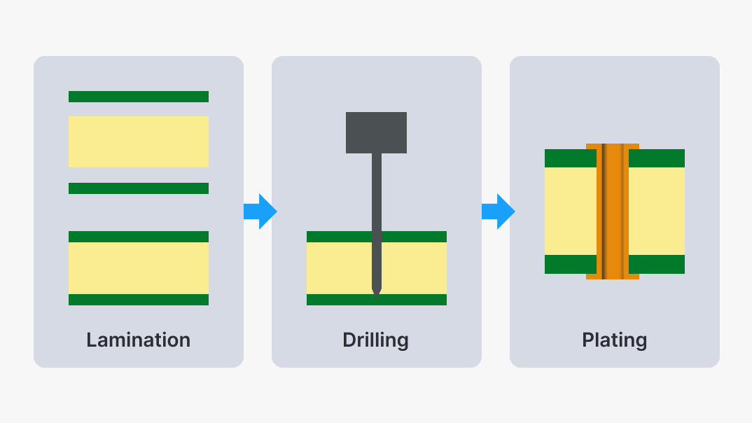
The Drill Checks procedure is used to produce comprehensive statistical data about the drill layers as well as to identify possible manufacturability flaws in the via, buried via, and blind via drill layers.This functionality only considers drill layers, specifically the top and bottom layers of a drill stack. It also makes use of any power or ground levels that exist in the stack. The checklist's core components are as follows:
| Check Items | Functions |
| Hole size | Provides a list of all PTHs, NPTHs & vias, and NPTHs that need pilot drills. |
| Hole separation | Reports duplicate holes, touching holes and close holes. |
| Missing holes | Reports missing drills for non-SMD pads. |
| Extra holes | Reports redundant drills that do not belong to any pad. |
| Power/ Ground shorts | Reports drills touching large copper nets of more than one power or ground layer. |
| NPTH to Route | Reports drills that have the Tooling hole or Mounting hole attributes, and NPTHs that are close to the route path. |
| Stubbed vias | Reports cases of vias not connected to at least two copper layers. |
| Thermal connection | Reports the absence of thermals for Thru-hole pin drills and calculates the total copper area of thermal connections through all negative power, ground and mixed layers. |
Signal and Mixed Layer Checks
This function examines a signal or mixed layer for potential manufacturability flaws and produces associated statistics. Although the action may be applied to any type of layer, typical use is with signal layers above. It utilizes the specific layer and any NC layer (drill or route) that overlaps it. The primary items checked for include:
| Check Items | Functions |
| Spacing | Reports spacing violations between pads, circuits and nets, and between text to text, also shorts and spacing between different CAD nets & close distances between non-touching features on the same CAD or layer nets. |
| Drill | Reports distance violations between NPTHs/PTHs/Vias, and pads, circuits, annular rings and copper. Also reports missing pads. |
| Route | Reports distance violations between edge of route features and pads, circuits, etc. |
| Size | Reports size of pads, shaved lines, text, line neckdowns, arcs and shaved arcs. |
| Sliver | Reports on slivers between lines and pads & between pads and pads. Slivers between a text feature & a functional pad will be reported, while silver between two features with the Copper Text attribute will be ignored. |
| Stubs | Reports unconnected line endpoints. |
Power/Ground Checks

The Power/Ground Checks are intended to identify manufacturability-related defects in power, ground, and mixed layers. The tool includes advanced algorithms on both negative and positive power and ground layers. Some of the key items on this major checklist include:
| Check Items | Functions |
| Drill | Reports distance violation between NPTHs/PTHs/Vias to plane, copper, clearance and annular rings. |
| Silver | Reports slivers in negative and positive layers. |
| Route | Reports close spacing between copper/clearance and route features |
| Thermal | Reports spoke (tie) widths and reduction of connectivity of thermal pads. |
| NFP Spacing | Reports spacing between NFPs and NFPs, NFPs and planes. |
| Plane spacing | Reports spacing between features of different planes |
| Keepin/ Keepout areas | Reports features inside/outside Keepin/Keepout areas |
| Plane width | Reports insufficient width of copper between 2 drills connected to a copper plane. |
| Plane connection | Reports disconnected areas of copper often used as reference planes that are left in a design could cause an unreferenced critical net, or a missing electrical connection. |
Solder Mask Checks
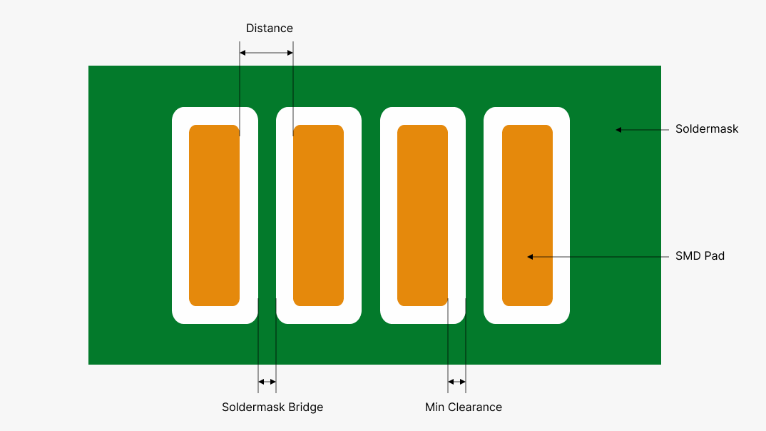
This function is aimed to check Solder Mask layers for possible manufacturability defects. Solder Mask layers are always considered negative; all positive features in the layer represent clearances or no solder mask. Additionally, the application of solder paste to every SMD pad will be verified, and one Solder Mask layer on each side is checked at a time. If more than one SMD layer is selected, this function will not perform properly. Following is the main checklist:
| Check Items | Functions |
| Drill | Reports close distance to solder mask openings of PTH/NPTH annular rings, and where NPTH touches mask.. |
| Pads | Reports close distance to solder mask openings of all pads, including undrilled pads. It also reports on a special group, Gaskets, which reports the width of solder mask overlap on features. |
| Coverage | Reports lines too close to clearance (that is, not adequately covered). |
| Route | Reports close distance between solder mask and route features. |
| Bridge | Reports different net pads without solder mask bridges. |
| Silver | Reports slivers between solder mask clearance. |
| Missing | Reports missing clearances. |
| Spacing | Reports close spacing between clearance (wider than silver). |
| Extra | Reports solder mask features which lack copper pads, or do not intersect with copper. |
Silkscreen Checks

This feature finds potential production issues within silkscreen layers and reports related statistics. This check applies only to silkscreen layers; however, it uses the job matrix to refer to external copper, solder mask, and drill layers. The key checklist covers the following:
| Check Items | Functions |
| Solder mask clearance | Reports close distances between silkscreen features and solder mask clearance. |
| SMD clearance | Reports close distances between silkscreen features and SMD pads. |
| Pad clearance | Reports close distances between silkscreen features and pads. |
| Hole clearance | Reports close distances between silkscreen features and drills. |
| Route clearance | Reports close distances between silkscreen features and route features. |
| Line width | Reports line width violations and length to width ratio violations. |
| String overlap | Reports the touching or intersection of silkscreen features of various string value. |
PCBX Provides Free DFM Check
Would you like to receive a free DFM or Design for Manufacturability check? Our Standard PCB service and Circuit Assembly service now include a free DFM check. Get free quotes today and get started.