Impedance Control
As circuit design becomes more complex and high-speed, it is challenging to maintain signal integrity, especially for high-speed signals. Ensuring signal quality is crucial, requiring transmission line theory for analysis and precise characteristic impedance matching.
Inadequate impedance control can result in considerable signal reflection and distortion, leading to design failure. Common signals such as PCI bus, PCI-E bus, USB, Ethernet, DDR memory, and LVDS signals require impedance control. Achieving impedance control ultimately depends on PCB design, which imposes higher demands on PCB manufacturing processes.
What is Impedance Control?
Impedance, in the context of electrical engineering and circuit design, is a measure of how much a circuit resists the flow of alternating current (AC) at a given frequency. It is a complex quantity that combines both resistance (the real part) and reactance (the imaginary part), and it is typically denoted by the symbol \( Z \). The unit of impedance is the ohm (Ω).
Impedance Control refers to ensuring that the impedance value of conductors within a circuit board remains within a specific range to prevent signal distortion. Various factors such as etching, layer thickness, and wire width can cause variations in impedance value, affecting signal integrity. Therefore, for high-speed circuit board conductors, the impedance value must be controlled within a defined range, known as "Impedance Control."
The impedance of PCB traces is determined by their inductive and capacitive reactance, resistance, and conductance coefficients. The main factors influencing the impedance of PCB traces include:
- Width of the copper trace
- Thickness of the copper trace
- Dielectric constant of the dielectric material
- Thickness of the dielectric material
- Thickness of the pads
- Path of the ground line
- Surrounding traces
- The impedance range for PCB traces typically lies between 25 and 120 ohms.

Why is Impedance Control Important?
Excellent impedance control allows a PCB to operate faster, more stably, and with less power consumption, thus enhancing product value and stability.
In certain fields such as RF communication, telecommunications, high-quality analog video (e.g., DDR, HDMI, Gigabit Ethernet), and electronic devices using high-frequency signals above 100MHz, PCB circuit signals require specific impedance for proper functioning. During high-frequency signal transmission, PCB traces play a crucial role, with each point on each trace having a specific impedance value. If the impedance varies from one point to another, signal reflection occurs. These reflections travel in the opposite direction of signal transmission, altering the original signal integrity. The magnitude of reflection depends on the difference between the two impedances, and significant discrepancies can prevent the signal from functioning correctly. Therefore, impedance matching ensures that impedance remains consistent across the entire circuit board to protect transmitted data from damage and maintain signal clarity. PCB traces must have controlled, uniform impedance, with longer traces or higher frequencies requiring more adjustments to minimize signal distortion caused by reflections. Proper PCB design and layout are the first steps to improving signal integrity in PCB traces.
Differences Between Impedance And Resistance
Impedance (measured in ohms) is like resistance, but for AC circuits only. Resistance limits both DC and AC currents, while impedance only applies to AC. Think of impedance as a traffic light for AC signals, keeping them flowing smoothly.
| Feature | Resistance (R) | Impedance (Z) |
| Summation | Simple addition | Vector addition |
| Frequency Dependence | Not affected | Affected |
| Current vs Voltage | In phase | Out of phase (due to inductance/capacitance) |
Factors affecting Impedance
Factors that influence the impedance of a PCB trace include:
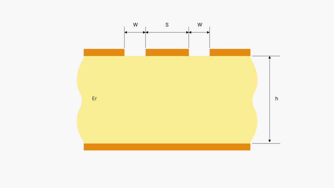
- The Width (w) and thickness (T) of the copper signal trace, both on the top and bottom layers.
- The Thickness (H) of the core or prepreg material positioned on either side of the copper trace.
- The Dielectric constant (εr) of both the core and prepreg materials.
- The Distance from other copper features on the PCB.
- In high-speed applications, such as signal processors, telecommunication, and RF transmission, the achievement of a controlled impedance is imperative.

How To Calculate Impedance Control?
Calculating impedance control for a PCB requires understanding several parameters and often involves complex equations or software simulations. Here's a step-by-step guide to get you started:
Determine Trace Dimensions:
- Trace Width (W): The width of the PCB trace.
- Trace Thickness (T): The thickness of the copper trace.
- Trace Length (L): The length of the trace, though it's not used directly in impedance calculations.
Determine Substrate Characteristics:
- Dielectric Constant (εr): The relative permittivity of the dielectric material (e.g., FR4).
- Dielectric Height (H): The height or thickness of the dielectric material between the trace and the reference plane.
Select the Impedance Model:
- Microstrip Model: When the trace is on the outer layer (surface) of the PCB.
- Stripline Model: When the trace is sandwiched between layers within the PCB.
Use Impedance Formulas:
- Microstrip Impedance (Surface Layer):
- For a microstrip, the characteristic impedance \( Z_0 \) can be approximated using the following formula:

- Stripline Impedance (Buried Layer):
- For a stripline, the characteristic impedance \( Z_0 \) can be calculated using:


