

PCB Fabrication
The complex process of designing a PCB (Printed Circuit Board) starts with a basic notion and ends with a fully functional PCB assembly. A schematic first records the net connectivity, and then a PCB designer puts the circuitry to optimize electrical properties within design restrictions. The circuit board is assembled into the system when the components are soldered to the board and the assembly testing and verification are complete.
There are several intricate procedures that need to be precisely followed in order to guide a circuit board from conception to completion. One of the most critical aspects of this process, which tends to be overlooked, is the fabrication of the bare board. Except for the design community, the circuit board fabrication process is somewhat mysterious and unknown. In contrast, the design phase of a PCB receives the most attention due in part to the sophisticated software programs used, and the manufacturing phase is praised for the joy of having a finished product.
To understand where an incomplete circuit board originated from and how it was readied for component installation, we must first examine the PCB creation process. In this way, we'll see what it takes to produce a quality circuit board fabrication the manufacturer can assemble seamlessly.
Basic Pre-Requisites of PCB Fabrication
PCB fabrication is the construction of the bare board that will form the base of the final PCB assembly. To facilitate the same, a comprehensive checklist of design elements needs to be compiled before the blank board was produced. Some of the following are critical aspects that must be assured before the start of fabrication and the respective information that board vendors will request:
Circuit Board Specifications
Before starting a PCB design, it is critically important for the design team to work with partner manufacturers to define the specifications and configuration of the physical board. This information is needed for the design layout and to select the appropriate PCB fabrication vendor for the project. Some of the key information includes:
Layer Stackup and Board Configuration: The number of layers and the type required.
Controlled Impedance Layers: Specifications for signal integrity and impedance control.
Minimum Trace Width and Spacing: Used for electrical performance and manufacturability.
Via Types and Structures: Including through-hole, blind, and buried vias.
Copper Balancing: Used for ensuring even copper distribution to avoid warpage.
PCB Panelization Considerations: To optimize the layout for manufacturing efficiencies.
Final PCB Design
The design shall be complete to ensure the correctness of PCB manufacturing. A minor update of a component without synchronization between the schematic and layout might affect the footprint and require rework or revision. The following are some design items to check before finalizing the design and preparing for manufacturing:
Full Engineering Review: The circuitry must have undergone a comprehensive review.
Schematic and Layout Synchronization: Both databases must be updated and synchronized.
Component Placement and Netlist: All components must be placed and all connections routed.
Optimization: Simulation of the circuit, signal integrity, and power integrity analysis.
Design Rule Check: Run DRC and correct all errors so that there are no violations.
Bill of Materials Review: Check the present availability and accuracy of the listed components.
Design for manufacturing Rules: Include DFM rules so that there are no assembly mistakes.
Complete Manufacturing Design Data
Once the design is fully developed and accessible, then comes the generation of fabrication and assembly data files to send to the contract manufacturer. They will use these files for their design reviews and forward the files to the fabrication vendor to get a quote and start production.
By meeting these very simple requirements, you can ensure smooth and effective PCB fabrication that, in turn, will set the stage for a successful final printed circuit board assembly.
PCB Fabrication Process: How to Create a Bare Board?
All this necessary design information and data is prepared, starting to produce the bare board. There are many types of circuit fabrications available, including single-sided boards, high-density multilayer designs, and flexible circuits. Here are the fabrication steps for a standard multilayer circuit board.
Creating Circuit Images

The first step in the circuit board fabrication process is to transfer the PCB design circuit image data from the files supplied by the CM to the board. Typically, this data comes in the common file format known as Gerber, as well as other formats and databases are available. There are two methods of transferring image data to the board:
Photo Tooling: This is the standard imaging process that has been used as long as there have been mass-produced circuit boards. A precision photoplotter creates the circuitry images on film, which then serves as a template for image printing in the fabrication process.
Direct Imaging: The circuit images are printed directly to the circuit board using a laser, eliminating the requirement for photo tooling. There are certain advantages over film since it is more accurate, has no alignment issues, and does not require periodic cleaning to replace worn out films. However, each layer must be individually laser-printed, making it more expensive.
The Structure of a Multi-layer PCB
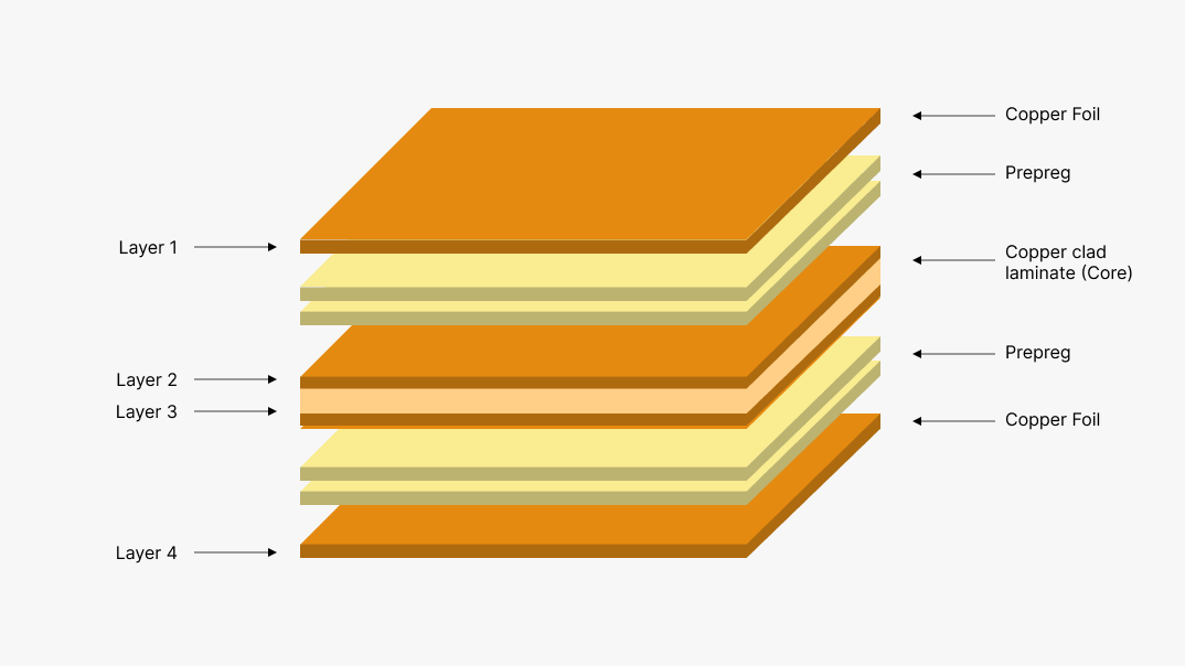
A multi-layer PCB consists of multiple layers of dielectric materials and metal conductors, and each layer pairs consist of a dielectric core material, usually epoxy resin and glass fiber commonly referred to as FR-4, sandwiched between two layers of copper foil. Although there are other dielectric materials available, FR-4 is still by far the most common core material used in making PCBs.
A multi-layer PCB is constructed by laminating multiple thinner versions of the same core structure as used in the double-sided board with other core structures for the overall board layer to stack up. Each layer must be strictly controlled for width and copper weight, and the alignment between the layers must be accurate for a good final product.
Inner Layer Circuit Fabrication
Printing images of circuit onto inner layer cores is the first step in making a PCB. Inner layer manufacturing includes the following steps:
Apply Photoresist: A sheet of photoresist material is laid over the copper foil of the core.
Expose: This photoresist is then exposed to ultraviolet light, utilizing photo tooling, or directly imaged by a laser. Exposure only occurs in the copper circuitry areas—pads and traces—where the photoresist over the circuitry patterns polymerizes and hardens.
Etching: Next, the copper layers of the core are etched to leave behind only the copper areas coated with the photoresist.
Stripping: The photoresist is then stripped, leaving behind only the intended copper circuitry.
After finishing all these steps, the core layers are sent for inspection by the AOI system to check for defects. Once every inner layer pair has successfully gone through this sequence, they will be prepared for lamination into a complete circuit board.
Laminating the Layers Together
Layer pairs are laminated together to create a PCB "sandwich." In between each layer pair, a sheet of "prepreg" is inserted to aid in the bonding of the layers. Prepreg is merely a fiberglass material impregnated with epoxy resin that melts under the heat and pressure of the lamination process. As the prepreg cools, it bonds the layer pairs together. Everything has to be perfect in this step because the correct line-up of the circuitry on the different layers must be made. After that, the layers are laminated and the heat and pressure bond the layers into a single circuit board.
Drilling the Holes
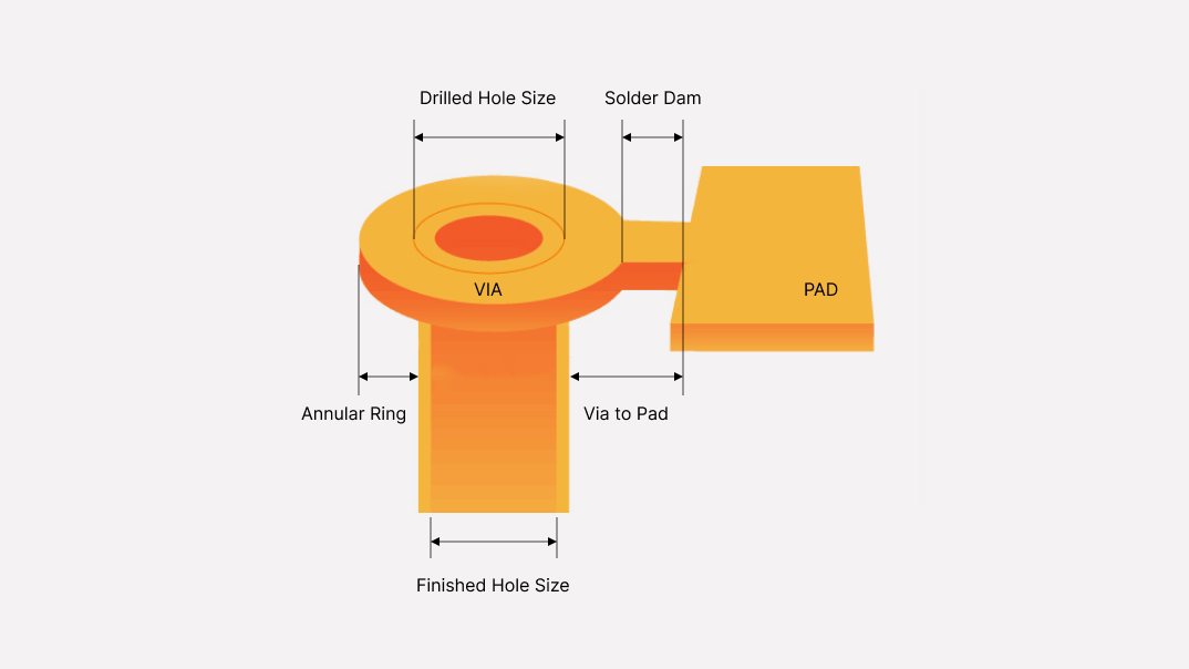
The next step in the fabrication process involves drilling the board for component mounting holes, thru-hole vias, and non-plated holes for any mechanical features. Most of the through-holes used in a circuit board need plating for electrical conductivity. Those through-holes are usually 0.005" larger than the specified finished hole size to allow for plating. If blind and buried vias or laser-drilled micro vias are part of the design, they necessitate individual drill-and-laminate cycles before the final lamination of the board. All of these many extra steps for sophisticated vias add to the fabrication cost but may be needed for High-Density Interconnect or improved electrical performance.
The holes are cleaned using both chemical and mechanical methods to remove resin smears and drilling debris. The entire exposed surface of the board, including the interiors of the drilled holes, is then chemically plated with a thin layer of copper to provide a metallic base for electroplating additional copper, both in the holes and on the outer layers.
Building the Top and Bottom Layer Circuitry
Now, the board is ready for its top and bottom circuitry images to be printed. This process is very similar to the photoresist application that was used for the inner layers but with one major difference: the circuitry will not be protected and must be built up with additional plating of copper.
Applying Photoresist: A sheet of photoresist material is applied to the top and bottom surfaces of the board, including the holes that are to be plated.
Exposure: The photoresist is exposed to UV light or a laser. Unlike the inner layers, the surface areas of the board do not have photoresist coverage over them except for the circuitry patterns.
Cleaning: The unexposed photoresist is cleaned away chemically, leaving bare copper circuitry patterns.
Plating: The exposed copper circuitry patterns have copper electroplated over them, adding to their metal weight.
Tin Plating: A layer of tin is then plated over the copper circuitry to protect it from oxidation. The photoresist is then stripped off of the rest of the board in preparation for etching.
Etching: Etching removes all of the copper from the board except for areas protected by the tin-plated circuitry.
Tin Removal: The tin is removed, leaving behind the finished, plated copper pads, traces, and through holes.
The printed circuitry on the top and bottom layers is now finished.
Solder Mask, Silkscreen, and Surface Finishes
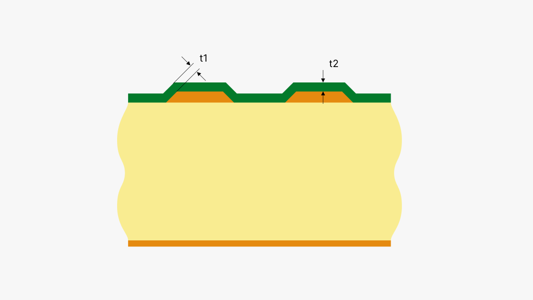
A solder mask is applied to the board to protect it during assembly, similar to the photoresist application process, with the solder mask material being applied to the entire board surface except for the metal pads and features intended for soldering. Other features silk-screened on a board include the component reference designators and other markings. The solder mask and silkscreen ink are cured through a baking process in an oven.
A surface finish is applied to the circuit board on the exposed metal areas. The surface finish protects the metal as well as aids in the soldering process during assembly. One type of surface finish is hot air solder leveling or HASL. During this process, the board is first fluxed to prepare it for soldering, and then it goes through a bath of molten solder. As the board leaves the solder bath, a high-pressure blast of hot air strips the excess solder from the holes and smoothes the solder on the surface metal.
Assembly Preparation, Inspection, and Testing
The final operation in PCB manufacturing is to prepare the circuit board for assembly. If needed, the circuit boards may be routed out from their manufacturing panels, or they may remain in the panel and be broken out after assembly. Depanellization means that a V-cut is scored along the board outline or the board is routed out, leaving small breakout tabs.
The completed board is then tested for continuity using automated test equipment, (nail bed test fixture or a flying probe test system), looking for any unexpected shorts between nets that could render the board invalid. After testing is completed and the board passes all of the inspections, it is returned to the PCB manufacturer for component assembly.
Need to Make Your PCB? PCBX Can Help!
The production process of PCB involves a great deal of intensive work. Therefore, to make sure your PCBs live up to your expectations for quality, performance, and longevity, you need to choose a manufacturer with a high degree of experience and a firm dedication to quality at every step.
PCBX is one of the most experienced service providers for the production of custom PCBs in China. We strongly believe that our success is determined by the success of our clients, taking great care and attention to detail during the entire PCB fabrication process. Besides, with vacuum packaging, weighing, and delivery to ensure your PCB order arrives safely and undamaged.
We are offering quick-turn PCB prototyping, mass PCB production, and assembly services. Fast and FREE quotations are always available. So far, we have been served for companies of all-size PCB in over 80 countries, and in the coming years, we hope to supply our PCBs to every corner of the world.