

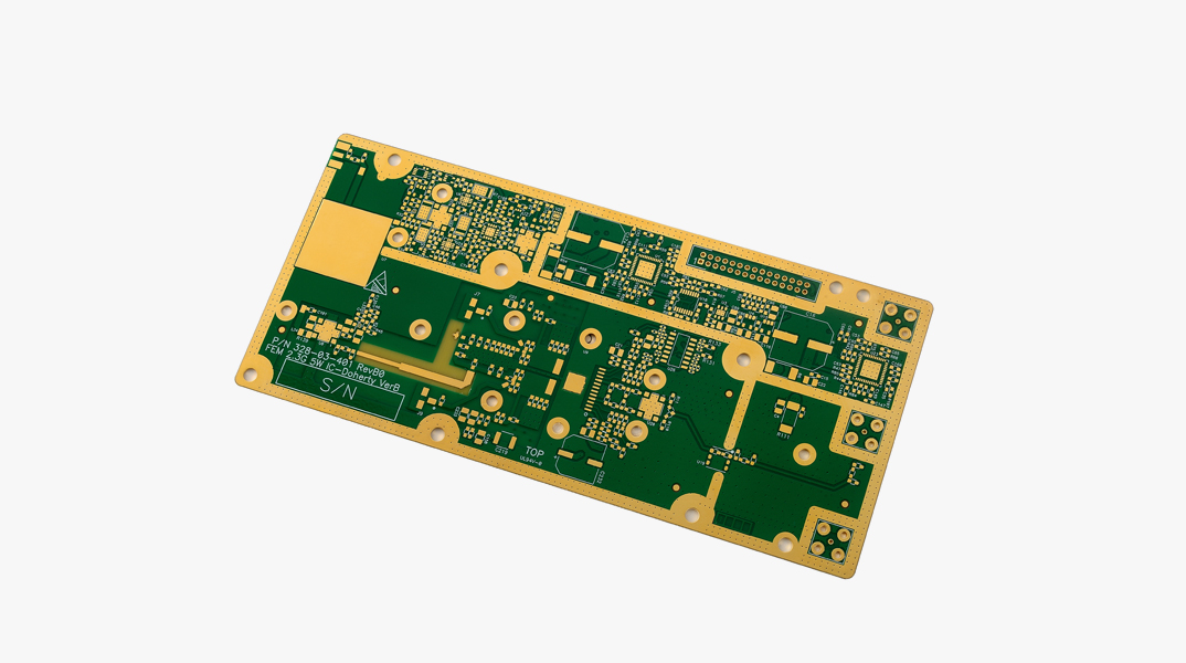
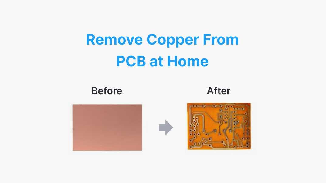
PCB Manufacturing Process
Printed Circuit Boards (PCBs) form the necessary framework in advanced electronics, fulfilling both electrical and mechanical demands by routing the electrical signals across the components. This intricate web of copper circuits makes sure that each component has seamless performance. Here is a detailed professional guide into the steps of the PCB manufacturing process:
PCB Manufacturing Process Steps
Design and Output
For creating the layout of the printed circuit board, a designer uses special design software, such as Altium Designer, OrCAD, Pads, KiCad, or Eagle. It is very important to inform the contract manufacturer of the exact software version used to create the design file to avoid mismatch.
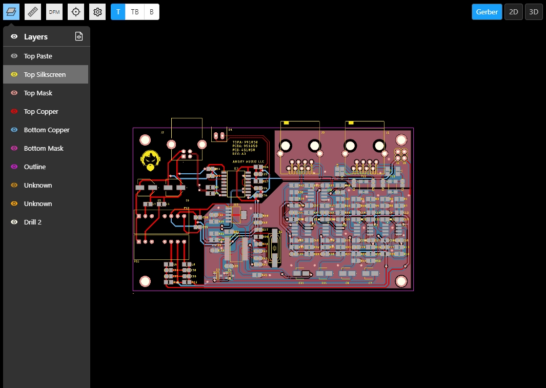
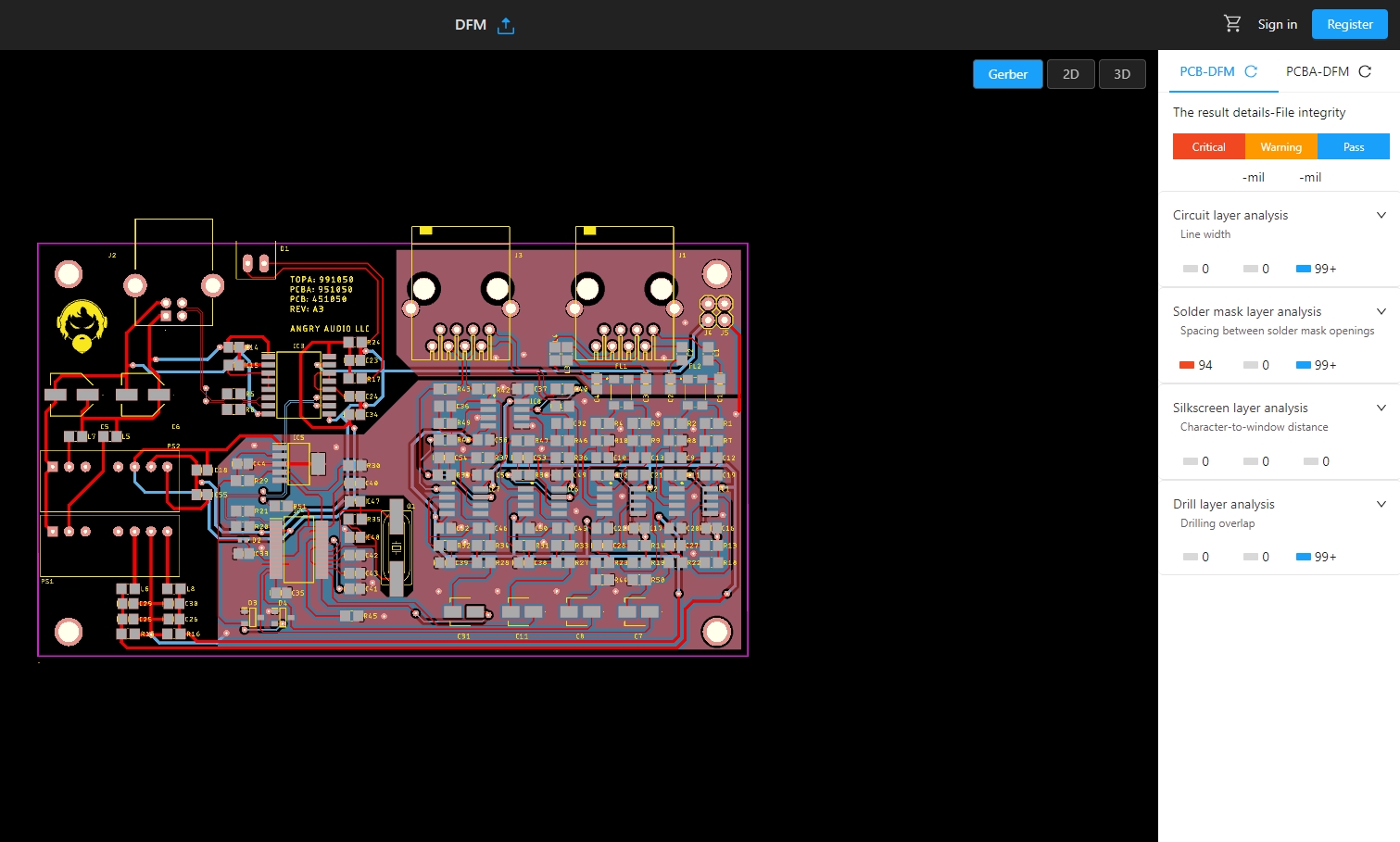
From the file, the final design is exported in a manufacturer-supported format, usually the extended Gerber. It represents a compressed format of the critical data, containing copper tracking layers, drill plans, aperture details, and notations for components. Strict checks ensconced in the design include track width, board edge spacing, trace size, and hole to hole spacing. The design files are sent to a PCB fabrication facility, which sometimes arranges to have their DFM checks made to ensure their capability for manufacture has a tolerance capable of outturning the design.
From File to Film
When designers output the PCB schematic files and manufacturers check for DFM, the PCB printing process begins. Manufacturers use special printers called plotters which print photo films of the PCB layout in detail. The high-precision plotters create plastic sheets that show a photograph negative of the PCB design in black ink.
For inner layers, the black ink is used for conductive copper parts, and the white/blank area is part of the non-conductive layer. It's the reverse for the outer layers. The films are 'self-developed' and considered precious, so they are not allowed to touch each other. Registration holes are punched to align the layers in future imaging processes.
Inner Layers Printed: Copper Deposition Process
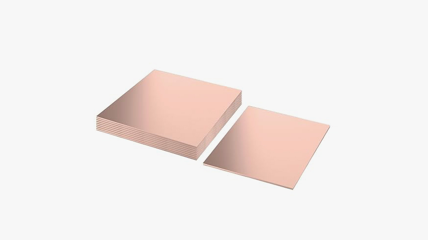
This stage would be one whereby the film design is transferred to copper foil. The material that substrates will have in common is a laminate board composed of epoxy resin and glass fibre, to supply a dust-free, stable base for laying down the copper.
Cleanliness must be strictly observed during this step; the laminate, which is coated with a copper side, is cleaned and processed under a decontaminated environment. A certain chemical film, which is photo-sensitive, called photoresist is coated to it, thus when hit with UV, light hardens the photoresist. The composite design of the PCB board is transferred to the laminate through the photoresist film. Photoresist that was not exposed to the light is rinsed off, leaving the supposed copper portions hardened.
Eliminate Photoresist Residual
This is the time of photoresist residual elimination in order to leave behind only the copper to be in the final circuit. An intense chemical solution dissolves excessive copper, while that which is protected in a mask will remain. Then, further solvents take away cured photoresists to reveal the copper substrate that is crucial to the PCB.
Layer Alignment and Optical Inspection
The alignment punches and an optical punch machine assure proper internal and external alignment of the different layers of the PCB. Automatic optical inspection then occurs via a laser sensor that will scan each layer against the original Gerber files; discrepancies are flagged for a technician to check.
Layer Up and Bond
This step involves combining and bonding the layers of the PCB. Copper foil and prepreg fiberglass sheets are made up as a laminate on either side of the substrate. The laminate is then assembled onto a steel table with metal clamps and alignment pins. Pressure and heating cycles bond these layers with a computer-controlled bonding press into a single unit.
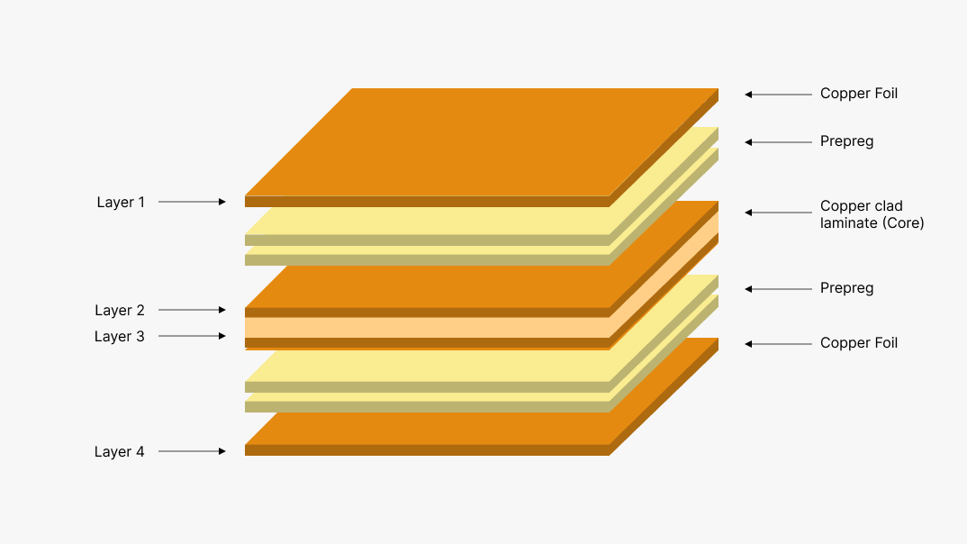
The next process removes the restraining pins and all excess plates uncovers the bonded copper foil on just the outer layers.
Drilling
This is where components and vías have precision holes drilled by computer-controlled drill machines. This machine has x-ray locators in order to locate the drill correctly. Computer-controlled drill machine is used to make high speed air driven spindles in order to bore holes of diameters of up to 100 microns, this is facilitated by buffer boards which ensure the exits of the drills are clean.
Plating and Copper Deposition
Chemical deposition plates the drilled panels with copper, thus forming conductive paths through the layers of a PCB. The panels are then cleaned and subjected to various chemical treatments. Copper baths deposit a thin layer of copper, covering the whole drilled holes and surfaces of the panel. All those steps are controlled by computers so as to have consistency.
This step is the same as the inner layer imaging step, but it is applied to outer layers. Photoresist coated in a clean room is exposed to ultraviolet light through black ink photo tools, hardening in areas where it is needed. The unhardened photoresist is removed, and the layer is ready for further processing.
Outer Layer Imaging
This step replicates the inner layer imaging process but for outer layers. Photoresist applied in a sterile environment is exposed to UV light through black ink transparencies, hardening only where required. The unhardened photoresist is then removed, leaving the layer ready for further processing.
Electroplating
A thin layer of copper is applied to the exposed areas that were imaged in the previous step. The panels then are tin-plated to mask the copper areas that will not be etched away in the subsequent step, which takes away the rest of the copper foil.
Final Etching
Important conductive areas and interconnects are developed with controlled etching methods.
Solder Mask Application
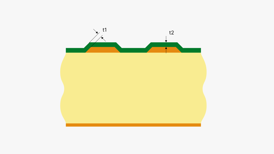
Apply an epoxy solder mask that is applied to the panels; it is exposed to UV light and then developed in the areas where the makers need exposure. Then, the panels are oven-cured.
Surface Finish
Surface finish, for example, gold or silver plating, which is done to the PCB's, improves their solderability. Through hot air leveling, the surface of the pads is standardized to a uniform finish.
Silkscreen
Ink-jet printing imparts vital information about the PCB onto the surface, and it is cured to stabilize the print.
Electrical Testing
Automated electrical tests are used to verify if a PCB works within its expected parameters and has the right design. More advanced testing methods include the Flying Probe Testing method; moving probes test the electrical performance of the board presented for testing.
Profiling and V-Scoring
At this stage, individual boards are separated from the main panel using routing or v-grooving methods for easier removal.
Choose PCBX for PCB Manufacturing
Manufacturing the best quality of PCBs requires a lot of knowledge and precision. As a leader among the Chinese custom PCB production service vendors, PCBX ensures top-quality samples for mass production and assembly. We promise on-time delivery and the greatest packaging to more than 80 countries.
For more information and consultation, please contact us directly. Quick and Free Quote is available.
Partnership with PCBX, you are assured of a reliable manufacturing process, quality, and performance of your PCBs meeting and exceeding the demands of durability.