X-Ray Inspection
What is X-Ray Inspection?
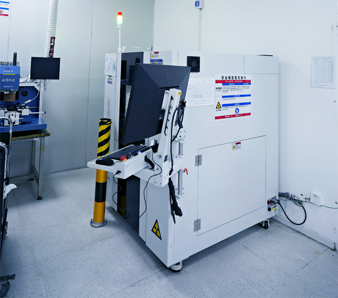
X-ray detection technology, commonly referred to as Automated X-ray Inspection (AXI), is a non-destructive method that utilizes X-rays to examine the hidden features of target objects or products. Its ability to penetrate through various materials makes it a valuable tool in a wide range of industries, including medicine, industrial control, and aerospace. In the realm of PCB (Printed Circuit Board) inspection, X-ray technology plays a crucial role in ensuring quality during the assembly process.
This is particularly important for modern PCBs with intricate designs, dense components, and multiple layers, where traditional inspection methods often fall short in detecting hidden defects.
Now let's explore its function and how to choose the right inspection.

How Does X-Ray Inspection Systems Work?
X-ray for PCB inspection allows the examination of features that traditional methods such as microscopes and Automated Optical Inspection (AOI) cannot reveal, which enables the inspection of components and soldering issues on PCBs.
X-Ray Inspection of Electronic Components
SMT components, like BGAs (Ball Grid Arrays), QFNs (Quad Flat No-leads), or complex ICs (Integrated Circuits), can be challenging to inspect visually because their connections are typically located underneath the package and are almost inaccessible, which necessitates the use of X-ray technology. SMT X-ray inspection is commonly utilized to detect the following defects:
- Missing components
- Misaligned components
- Damaged components
- Incorrect component values
- Lifted pins or leads
- Component defects, such as misalignment, usually manifest as a mismatch between the shadows of the pins and the pads. Other defects are similarly detected by observing the bright and dark areas and recognizing distinct anomalies.
X-Ray Solder Joint Inspection
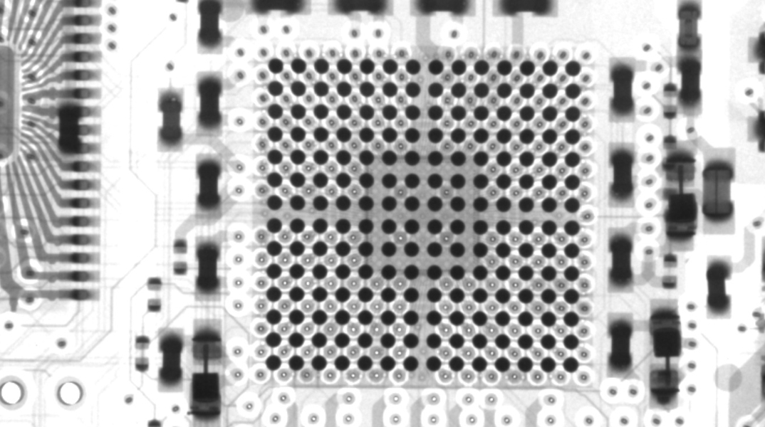
X-rays are readily absorbed by the dense materials in solder alloys. As a result, the solder appears darker than other parts of the circuit board, including components and the core or substrate. During PCB X-ray inspection, the dark color of the solder helps in identifying the following issues:
- Solder voids
- Solder bridges
- Insufficient solder
- Excessive solder
- Solder quality
- Solder shorts
- For instance, a dark bridge (grey) between solder joints might indicate a solder short, while brighter spots within the soldered parts may signify voids. Insufficient solder, among other defects, is also identified as a bright spot in the circuitry.

X-RAY Inspection Image
- Behind the Scenes: The X-ray Inspection Trio
- X-ray inspection equipment is a well-coordinated team of three:
- X-ray Tube: This acts as the source, generating X-rays by bombarding a metal target with high-speed electrons.
- Sample Handling Platform: This robotic stage precisely maneuvers the PCB, ensuring X-rays can scan it from multiple angles, leaving no hidden corners unexamined.
- Detector: Located on the opposite side of the PCB, the detector captures the X-rays that pass through and translates them into a digital image. This image can be a simple 2D representation or a sophisticated 3D model, depending on the system's capabilities.
Advantages of X-Ray Inspection
- Non-destructive: X-ray inspection is non-intrusive and non-destructive. During the process, no part of the circuit board or its assembled components is damaged or destroyed.
- Hidden Defects: Unlike visual methods, X-ray PCB inspection can help reveal hidden parts of the circuit board, such as inner layers or BGA and IC connections.
- Flexible Examination: X-ray inspection can create 2D or 3D views of PCB structures, providing the flexibility needed to analyze different types of circuit boards based on the required level of visualization.
- Higher Accuracy: Compared to other technologies like magnifiers, microscopes, and automated optical inspection (AOI), X-ray PCB inspection offers higher accuracy. It provides a clear analysis of solder joints, component connections, and other critical information needed for thorough inspection.
- Failure Analysis: Using information obtained from X-ray inspection, engineers can analyze defects and effectively determine their root causes. This leads to improved PCB quality based on actual improvements.
How to Choose the Right Inspection Method?
A significant advancement in Automated X-ray Inspection (AXI) is the incorporation of 3D technology, complementing existing 2D methods and enhancing performance. Selecting the appropriate inspection method, whether AOI or AXI, for defect classification, can be challenging. The following charts offer guidance in making this choice.
| Defect Type | AXI | AOI |
| Soldering defects | ||
| Open circuits | Y | Y |
| Solder bridges | Y | Y |
| Solder shorts | Y | Y |
| Insufficient solder | Y | Y |
| Solder void | Y | N |
| Excess solder | Y | Y |
| Solder quality | Y | N |
| Component defects | ||
| Lifted lead | Y | Y |
| Missing component | Y | Y |
| Misaligned/misplaced component | Y | Y |
| Incorrect component value | N | N |
| Faulty component | N | N |
| BGA and CSP defects | ||
| BGA shorts | Y | N |
| BGA open circuit connections | Y | N |
Briefly, PCB X-ray inspection is a powerful technique that allows for the visualization of hidden defects, ensuring high-quality PCB production. Integrating X-ray inspection into the production line offers flexibility, enabling 2D or 3D views and varying radiation levels for comprehensive analysis.


