- Products & Capabilities

- Simulation Design & EDA

- About
- Resources
PCBX.com Resources
Your source for industry knowledge, news, and expert insights

Latest Posts
Article
PCB slots, essential in design and performance, aid in electrical connection and heat dissipation. Both plated and non-plated types serve specific applications.
 2024/12/19
PCB plates enhance electronic devices' structure and function, crucial in keyboards for stability and connectivity. Materials and designs aid efficient decisions.
2024/11/25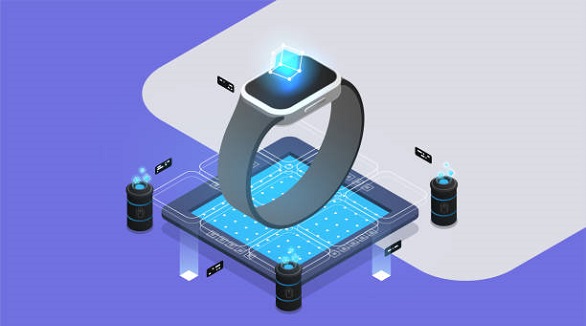
Smartwatches enhance life with health, connectivity, and safety features, supported by tech advances and ecosystem integration, driving market growth.
2024/11/20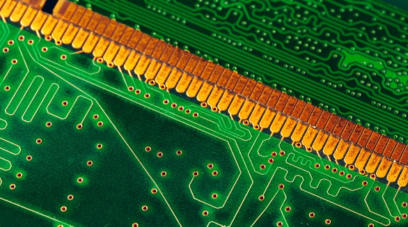
Gold finishing on PCBs, using immersion or plating, protects against oxidation and enhances solderability. Immersion is cheaper for intricate designs, while plating is durable for high-reliability needs.
2024/10/18
Understanding PCB current ratings ensures safe electric flow. Optimize trace size, copper weight, and use via calculators and high-current connectors for efficient and reliable PCB designs.
2024/10/17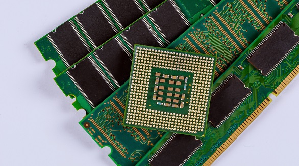
Gold plating in PCB manufacturing increases electrical properties, durability, and corrosion resistance, ideal for high-reliability applications. Types include ENIG (common, flat, solderable) and ENG (thicker, durable).
2024/09/20PCB side plating, or edge plating, involves copper along PCB edges, enhancing connectivity, conductivity, shock protection, and assembly, especially for small boards. Used in Wi-Fi and Bluetooth modules, it improves signal quality and EMC. Limitations include necessary design gaps and exclusion of V-cuts.
2024/08/21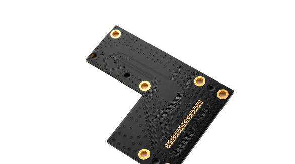
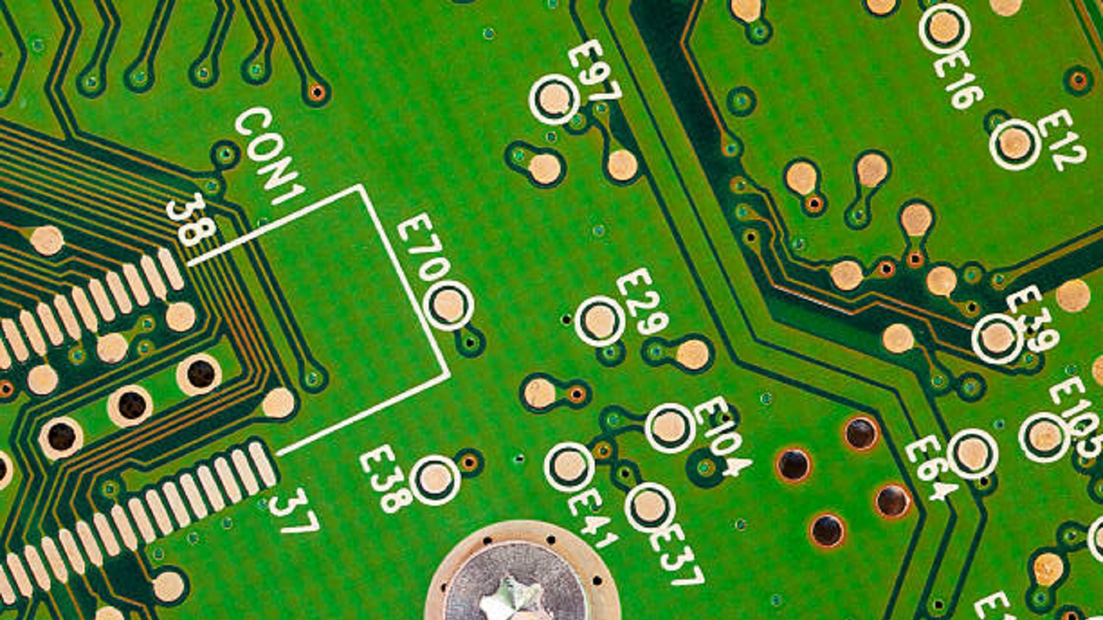
Plated-through slots (PTS) in PCBs are copper-plated apertures for electrical connectivity, offering space optimization, reduced soldering voids, and improved surface use.
2024/08/06