- Products & Capabilities

- Simulation Design & EDA

- About
- Resources
PCBX.com Resources
Your source for industry knowledge, news, and expert insights

Latest Posts
Article
Mounting power supplies on PCBs optimizes space, reliability, and performance. Key factors include layout, thermal management, and mounting methods.
 2025/02/07
Reduce PCB noise for reliable analog signals with organized design, strategic layout, component selection, and targeted noise management techniques to enhance performance.
2025/02/05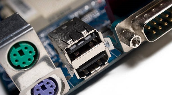
PCB insertion loss is crucial to managing signal attenuation in high-frequency designs, affected by materials, path length, and connectors—optimized through strategic design measures.
2025/01/16
PCB aspect ratio, relating board thickness to via diameter, is key for quality, cost, and reliability in manufacturing, impacting plating and design.
2025/01/02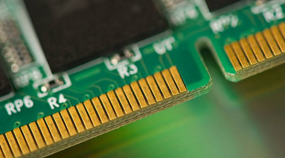
Edge connector bevelling enhances PCB durability and reliable connections, vital for frequent usage and secure engagements, with limitations primarily in plating.
2024/12/25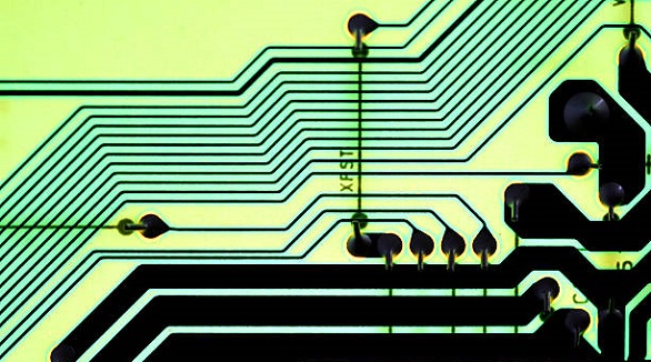
PCB design hinges on safe spacing for reliability; it prevents short circuits and ensures durability, addressing both electrical and non-electrical factors.
2024/12/25
10 oz copper PCBs offer high current capacity, improved thermal management, and durability for demanding applications in power electronics, aerospace, and military.
2024/12/20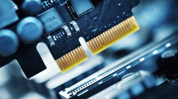
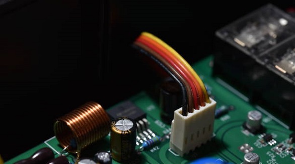
PCB connectors are crucial for reliable connections in electronics, enabling effective performance across various industries through careful selection and maintenance.
2024/11/29