PCBX.com Resources
Your source for industry knowledge, news, and expert insights

Latest Posts
Article

Selective soldering offers precision and efficiency for complex PCB assemblies, targeting specific areas with improved quality, cost-effectiveness, and flexibility, overcoming limitations of wave soldering.

SMD soldering mounts small components on the PCB surface for compact, automated designs but has high setup costs and repair challenges. DIP soldering uses through-hole components for robust, easily repairable, lower-volume applications.

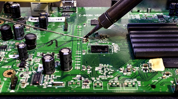
The article provides a step-by-step guide to soldering a PCB, covering workspace setup, essential tools, and safety measures. It explains heating the soldering iron, applying flux, tinning the iron tip, placing components, heating joints, applying solder, cooling, inspecting, and cleaning. Emphasis is on practice and safety for successful soldering.

Wave soldering quality hinges on several factors: consistent solder contact, precise heat management, optimal separation speed, and controlling solder surface tension. Key considerations include deoxidizing surfaces for effective wetting, strategic lead/pad design, and correct component orientation. Mastering these variables enhances PCB assembly reliability.
