- Products & Capabilities

- Simulation Design & EDA

- About
- Resources
PCBX.com Resources
Your source for industry knowledge, news, and expert insights

Latest Posts
Article
Superior PCBA testing ensures quality, functionality, and reliability, using diverse methods to prevent flaws, maintain standards, and enhance electronics manufacturing.
 2025/03/18
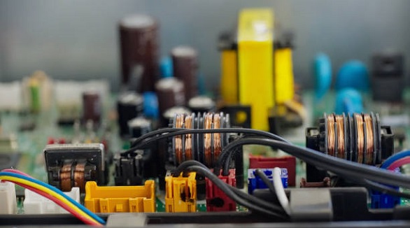
Rectifier diodes convert AC to DC, ensuring devices receive correct power, essential in electronics, from power supplies to battery chargers, with high efficiency.
2024/12/24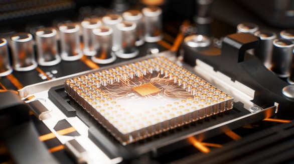
Package on Package (PoP) assembly stacks semiconductor devices vertically, enhancing space efficiency and performance in electronics with design flexibility.
2024/12/20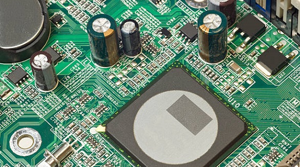
BGA rework stations offer precision, automation, and cost-efficiency, solving challenges in high-density electronics by optimizing component alignment and heating.
2024/12/19
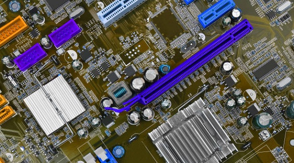
Populated circuit boards integrate electronic components for efficiency and reliability, utilizing SMT and THT for diverse applications across industries.
2024/12/17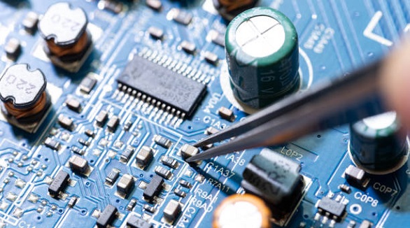
Master soldering chip components on PCBs using proper tools and techniques, ensuring precision and reliability for both hobbyists and professionals in electronics.
2024/12/03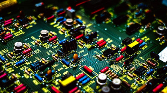
IC boards, integral to electronics, integrate circuits on PCBs, offering cost-effectiveness, miniaturization, and versatility across various technologies.
2024/11/20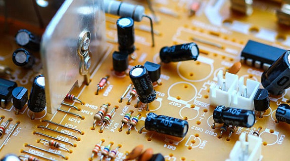
Capacitors must be safely discharged to prevent shock and damage. Use insulated tools, check voltage, and follow protocols to ensure safety during maintenance.
2024/11/18