- Products & Capabilities

- Simulation Design & EDA

- About
- Resources
PCBX.com Resources
Your source for industry knowledge, news, and expert insights

Latest Posts
Article
Serial numbers on PCBs are crucial for traceability, quality control, warranty support, and inventory management, ensuring compatibility and efficient device management.
 2025/03/27
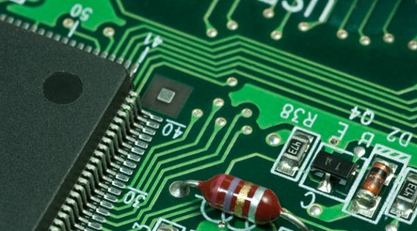
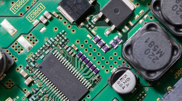
Current limiting circuits are crucial in PCB designs, preventing overcurrent damage and ensuring safe, reliable operation across various electronic applications.
2025/02/21
Pin in Paste (PiP) enables efficient, cost-effective PCB assembly, integrating through-hole and surface mount components in a single reflow pass, reducing costs.
2025/02/17
Microphone PCBs transform sound to electrical signals using ECM or MEMS tech, focusing on compact, efficient designs for high-fidelity audio applications.
2025/02/14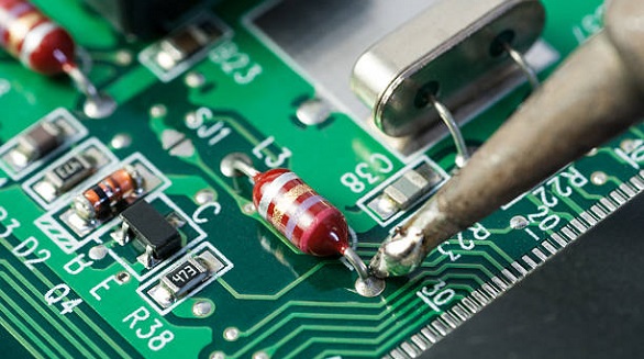
Dry solder joints in PCBs cause unreliable connections, leading to device failure. Prevent with proper heat, cleaning, quality solder, and skilled techniques.
2025/02/14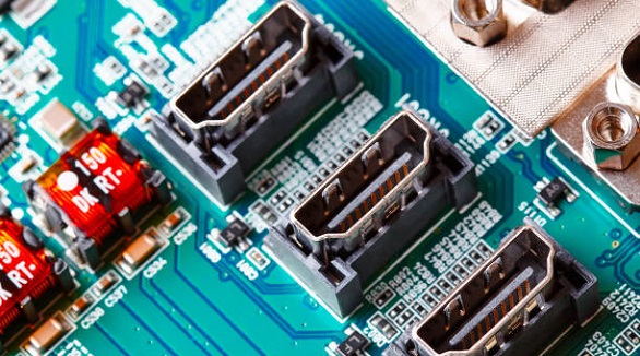
Start-stop circuits efficiently control devices, enhancing safety and performance in industrial and consumer applications through simple push-button mechanisms.
2025/02/13
Ground loop control in PCBs is essential to prevent EMI and signal degradation, using ground planes, star grounding, and isolating signal grounds.
2025/02/13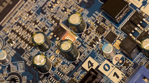
The 94V-0 circuit board ensures safety in electronics by meeting fire resistance standards, essential for compliance, reliability, and reduced liability in devices.
2025/02/12