- Products & Capabilities

- Simulation Design & EDA

- About
- Resources
PCBX.com Resources
Your source for industry knowledge, news, and expert insights

Latest Posts
Article
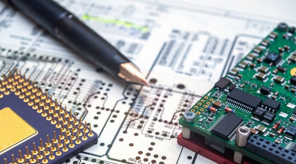
PCB design demands precision, using subcircuits for optimized layout, managing thermal concerns, and minimizing signal paths to ensure performance and manufacturability.
 2025/01/17
Castellated pads in PCB design facilitate easy board-to-board connections, enhancing miniaturization, assembly, solder quality, and flexibility for compact modules.
2025/01/13
Voltage regulator PCBs ensure stable electronic device operation, offering solutions like linear and switching regulators for efficiency and reliability in designs.
2025/01/10
Capacitors are crucial in PCB design for filtering and timing. Correct polarity in electrolytic and tantalum types prevents malfunctions and ensures reliability.
2025/01/09
The article highlights the top 10 wireless router manufacturers, including Cisco, Netgear, and TP-Link, emphasizing their performance, features, and target markets.
2024/12/27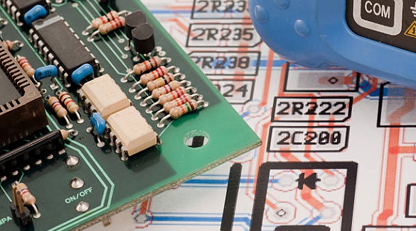
Diodes, basic yet essential, control current flow in circuits and are key in PCB design, aiding rectification, signal detection, and voltage regulation.
2024/12/27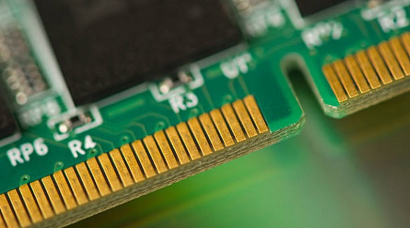
Edge connector bevelling enhances PCB durability and reliable connections, vital for frequent usage and secure engagements, with limitations primarily in plating.
2024/12/25
PCB design hinges on safe spacing for reliability; it prevents short circuits and ensures durability, addressing both electrical and non-electrical factors.
2024/12/25