- Products & Capabilities

- About
- Resources
PCBX.com Resources
Your source for industry knowledge, news, and expert insights

Latest Posts
Article
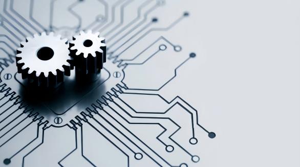
Embedded electronics design focuses on small, low-power specialized computing systems, covering their classification, workflow, applications, benefits, challenges and future trends in modern tech.
 2026/03/12
PCB thickness is essential for device performance, impacting signal integrity, thermal efficiency, and durability, thus requiring careful selection for optimal outcomes.
2026/01/27
Choosing the right dielectric material for aluminum PCBs ensures effective thermal management, insulation, and reliability in high-power applications like LED lighting and vehicles.
2026/01/08
Wave soldering fixtures are crucial for achieving precise through-hole PCB assembly, minimizing defects, and enhancing overall manufacturing efficiency.
2025/12/30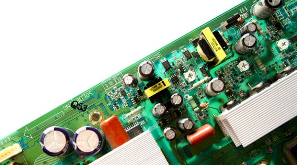
PCB failures due to minor orientation and polarity errors can impact reliability, but proper design practices and checks ensure manufacturability and performance.
2025/12/18
PCB panelization improves productivity, reduces costs, and facilitates automation by assembling several smaller PCBs into one large panel, ensuring uniformity.
2025/11/06
PCB footprints are essential for ensuring accurate component placement, electrical connections, and overall reliability, significantly impacting the manufacturability and performance of electronic devices.
2025/10/11
BGAs are vital for compact, high-functionality devices, but demand meticulous routing to overcome design challenges in reliability, manufacturability, and signal integrity.
2025/09/11