- Products & Capabilities

- Simulation Design & EDA

- About
- Resources
PCBX.com Resources
Your source for industry knowledge, news, and expert insights

Latest Posts
Article
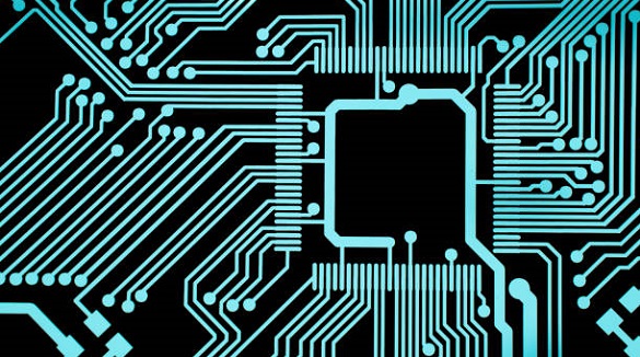
PCB layout design transforms schematics into reliable, efficient electronic products by optimizing signal integrity, power distribution, and thermal management.
 2025/06/04
In PCB manufacturing, DFM Checks ensure efficient production by identifying design issues early, reducing costs, enhancing quality, and preventing delays.
2025/05/20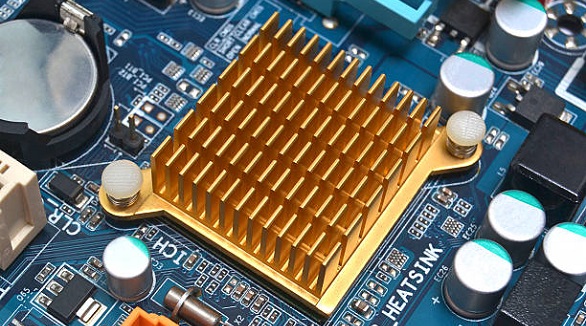
Heat sinks are essential for reliable PCB design, managing heat in high-density components like transistors and LEDs, ensuring optimal performance.
2025/02/06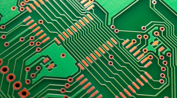
Controlled impedance is crucial in modern PCBs, ensuring signal integrity through precise trace and material design, essential for high-speed applications.
2025/01/24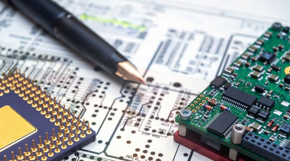
PCB design demands precision, using subcircuits for optimized layout, managing thermal concerns, and minimizing signal paths to ensure performance and manufacturability.
2025/01/17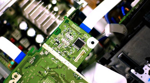
Castellated pads in PCB design facilitate easy board-to-board connections, enhancing miniaturization, assembly, solder quality, and flexibility for compact modules.
2025/01/13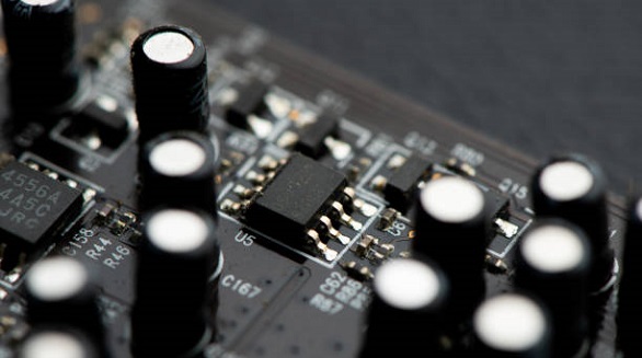
Voltage regulator PCBs ensure stable electronic device operation, offering solutions like linear and switching regulators for efficiency and reliability in designs.
2025/01/10
Capacitors are crucial in PCB design for filtering and timing. Correct polarity in electrolytic and tantalum types prevents malfunctions and ensures reliability.
2025/01/09