- Products & Capabilities

- Simulation Design & EDA

- About
- Resources
PCBX.com Resources
Your source for industry knowledge, news, and expert insights

Latest Posts
Article
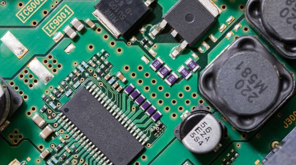
Serial numbers on PCBs are crucial for traceability, quality control, warranty support, and inventory management, ensuring compatibility and efficient device management.
 2025/03/27
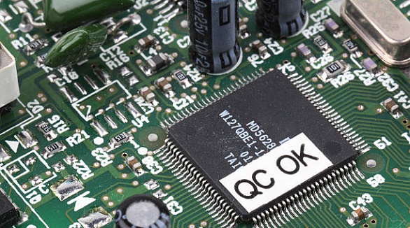
IPC-A-600 standard guides PCB quality through three class levels, ensuring durability and reliability for diverse applications, crucial for manufacturers.
2024/12/30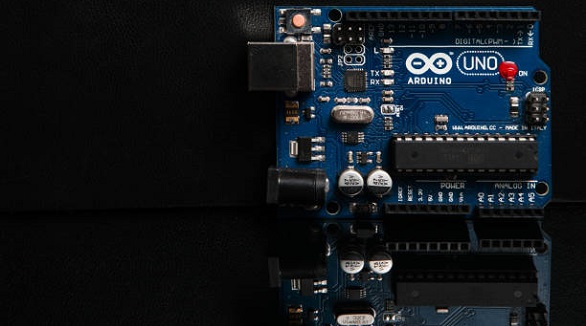
Arduino Leonardo and UNO both excel in electronics, with Leonardo suited for HID and USB projects, while UNO is cost-effective for beginners and simple tasks.
2024/11/27
Power and ground planes in PCBs ensure signal integrity, manage heat, and minimize EMI, crucial for efficient, high-performance electronic devices.
2024/11/11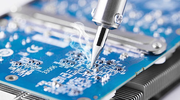
Solder flux ensures strong PCB joints by cleaning oxidation. Types include rosin, no-clean, and water-soluble, crucial for reliable electronics assembly.
2024/11/08
Smart switches revolutionize homes. Leading brands like TP-Link, Lutron, WeMo, Leviton, and GE innovate with seamless integration and smart technology.
2024/11/08
PCB pads connect components on circuit boards. Understanding through-hole, surface-mount, and BGA pads is key for effective PCB design and manufacturing.
2024/11/08
Backplane PCBs provide critical connectivity, stability, and efficient communication in complex systems, essential in data centers, telecom, and industrial automation.
2024/11/06